NOTICE
Damage to the module
If the outputs are overloaded, the heat can melt the contacts.
Therefore, for a demand factor of 100%, a max. current of I
out
= 0.25 A at X111, X222, X333:
Pin 2, must not be exceeded.
Technical data
Table 12-25 Electrical specication of the digital outputs
Digital outputs min. Standard max. Nominal
High-level voltage (U
H
) V
CC
- 3 V
1)
V
CC
24 V
Output current I
OUT
- - 250 mA
2)
-
Voltage with low level (U
L
) - - - Output open
Leakage current at low level - 50 μA 400 μA -
Signal delay time T
PHL
- 0.5 ms - -
Maximum switching frequency
Resistive load - - 100 Hz -
Inductive load - - 2 Hz -
Lamp - - 11 Hz -
1) U
H_typical
= V
CC
- I
OUT
× R
ON
V
CC
: Current operating voltage
I
OUT
: Output current
Maximum short-circuit current: 4 A (max. 100 μs, V
CC
= 24 V)
R
ON
: Maximum internal resistance = 0.4 Ω
2) For a simultaneity factor of 100% (all outputs active)
Incorrect connection causes neither high level nor destruction of the outputs.
12.2.4 Parameterization
12.2.4.1 Input / output images
Input image
The image comprises 2 slots (n, d ≙ start address):
• Slot 1: Digital inputs (DI)
– n+0 … n+8 (9 byte)
– X222.P3 - .P10 are rapid inputs
• Slot 2: Diagnostics: d+0 .. d+1
Connectable components
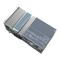
12.2 PP 72/48D PN
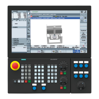
NCU 1740
124 Equipment Manual, 10/2021, A5E51087503B AA
 Loading...