3.4 Control Bus. The control bus is a collection of individual signals which supervise the flow of data on the address and data busses. The block
diagram shows most of these signals but reference to the circuit diagram shows other control signals available at the expansion port. Control lines
are summarised below.
3.5 Interrupt Control (IPL0/2, IPL1). These inputs indicate the encoded priority level of the device requesting an interrupt, and are fed by IC24 (pins
23, 24) and IC23 (pin 26). A satisfactory interrupt condition must exist for two successive clocks before triggering an internal interrupt request. An
interrupt acknowledge sequence is indicated by the function codes, FC0 and FC1. In this configuration FC0 and FC1 are NANDed together at
IC27,6 and the output routed to the valid peripheral address (VPA) input to the CPU. This input indicates that the processor should use automatic
vectoring for an interrupt. The IPL signals and VPA may also be input from an external device via J1, the main expansion connector.
3.6 A16 and A17. These two address bits select ZX8301 and are decoded by it to assert the relevant CAS0 and CAS1 signal and ROMOEH and
PCENL for the ZX8302 chip enable. For this purpose their states are either low and high, or high and low respectively. When ROM is being
addressed both are in the low state.
3.7 CLK Input. The CLK input denoted CLKCPU is the 7.5 MHz system clock from ZX8301. It is also fed to IC23 and IC24 and to the expansion
port connector.
3.8 Asynchronous data transfers are handled using the following control signals: DTACK, R/W, DS and AS. These signals are explained in the
following paragraphs.
3.9 DTACK (Data Transfer Acknowledge). This input indicates that the data transfer is completed, and is sent by the ZX8301 or through the
expansion connector. When the processor recognises DTACK during a read cycle, data is latched and the bus cycle is terminated. When DTACK
is recognised during a write cycle, the bus cycle is terminated.
3.10 R/W. This tri-state signal defines the data bus transfer as a read or write cycle. The R/W signal also works in conjunction with the data strobe
as explained in the following paragraph.
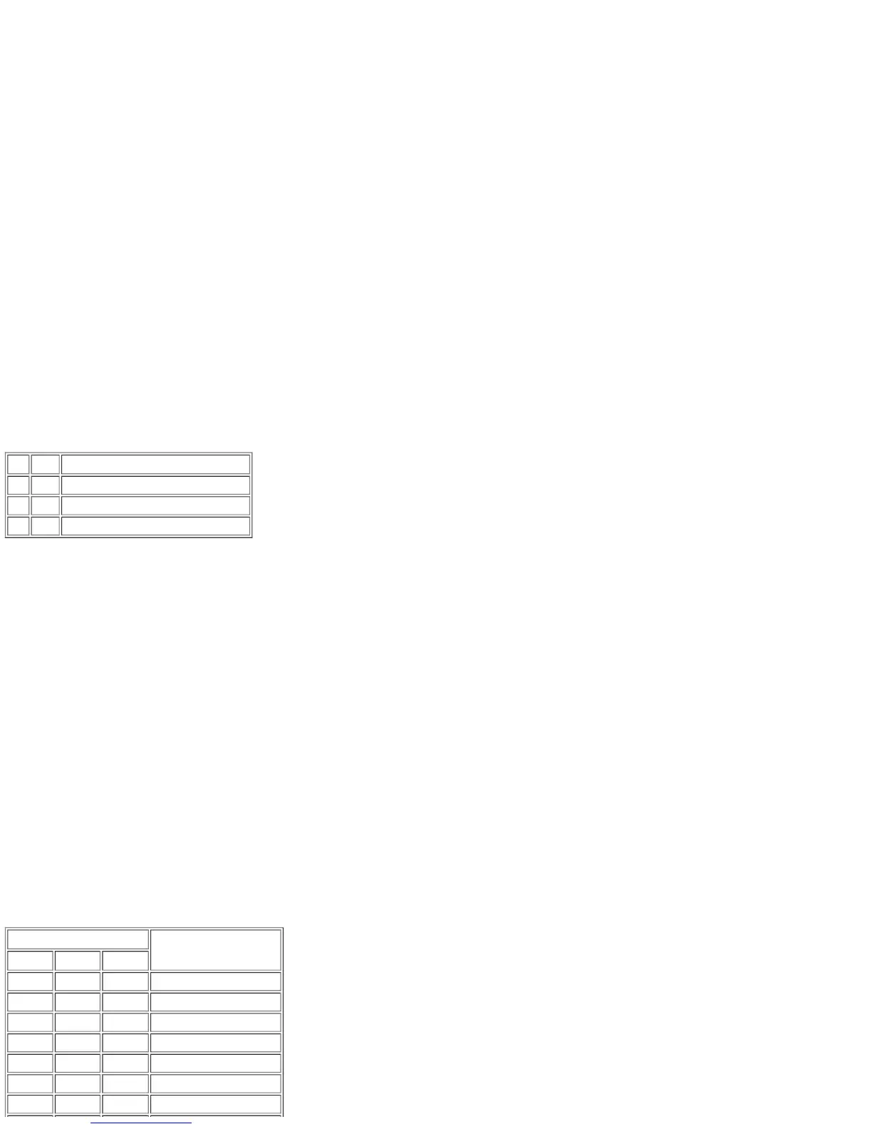
3.11 DS (Data Strobe). This tri-state signal controls the flow of data on the data bus as shown in the table below. When the R/W line is high, the
processor reads from the data bus as indicated. When the R/W line is low the processor writes to the data bus as shown.
DS R/W D0-D7
1 No valid data
0 1 Valid Data Bits 0-7 (Read Cycle)
0 0 Valid Data Bits 0-7 (Write Cycle)
If the CPU is addressing an external device with one of address bits A18 and A19 set, emitter follower TR8 is switched on by the signal KILLH from
IC38. This sets the DSMCL (Data Strobe Master Chip - Active Low; the 'Master Chip' is the ZX8301) line permanently high thus disabling IC23 and
IC22. The local DS signal is still enabled to J1, the expansion port, to control R/W operations from an external device. In the pre-Issue 6 version
TR8 is switched from IC18.
3.12 AS (Address Strobe). This tri-state signal indicates that there is a valid address on the address bus.
3.13 Four other groups of control signals are used by the CPU. These four groups are routed to J1 only and are associated with Bus Arbitration
Control, Peripheral Control, Processor Status and System Control in respect of external devices.
3.14 Bus Arbitration Control. An explanation of this function is included for information only. It is not used by the QL but could be used by
peripherals. The 68008 contains a simple 2-wire arbitration circuit designed to work with daisy-chained networks, priority encoded networks, or a
combination of these techniques. This circuit is used in determining which device will be the bus master device. The BR (Bus Request) input is wire
ORed with all other devices that could be bus masters. This device indicates to the processor that some other device desires to become the bus
master. Bus requests may be used at any time in a cycle or even if no cycle is being performed. The BG (Bus Grant) output signal indicates to all
other potential bus master devices that the processor will release bus control at the end of the current bus cycle.
3.15 M6800-compatible Peripheral Control is exercised through the VPA and E output lines. VPA is derived from two processor status signals
FC1 and FC0 as described above though this is only used for auto vectoring. E (Enable) is the standard enable signal common to all M6800 type
peripheral devices. The period for this output is 10 MC68008 clock periods (six clocks low, four clocks high).
3.16 Processor Status (FC0, FC1 and FC2) are function code outputs which indicate the state (user or supervisor) and the cycle type currently
being executed, as shown in the table below. The information indicated by the function code outputs is valid whenever address strobe (AS) is
active.
Function Code Output
Cycle Type
FC2 FC1 FC0
LOW LOW LOW (Undefined, Reserved)
LOW LOW HIGH User Data
LOW HIGH LOW User Program
LOW HIGH HIGH (Undefined, Reserved)
HIGH LOW LOW (Undefined, Reserved)
HIGH LOW HIGH Supervisor Data
HIGH HIGH LOW Supervisor Program