K850
1203-2528 rev. 1
APPENDIX Components D2420 - D2460
APPENDIX
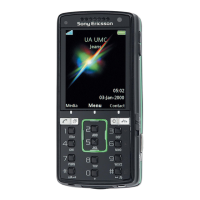
TQFN (4mm x 4mm)
TOP VIEW
MAX7327
19
20
21
22
12 3456
18 17 16 15 14 13
23
24
12
11
10
9
8
7
SCL
V+
SDA
INT
AD2
O0
+
O1
P2
P3
P4
P5
AD0
O15
O13
O12
O11
RST
O10
O8
O9
GND
O6
O7
O14
EXPOSED PADDLE
Pin Description
PIN
QSOP
TQFN
NOITCNUFEMAN
122 INT Active-Low Interrupt Output. INT is an open-drain output.
223 RST Active-Low Reset Input. Drive RST low to clear the 2-wire interface.
3, 21 24, 18
AD2, AD0
Address Inputs. Select device slave address with AD0 and AD2. Connect AD0 and AD2
to either GND, V+, SCL, or SDA to give four logic combinations (see Tables 2 and 3).
4, 5, 10,
11, 13–20
1, 2, 7, 8,
10–17
O0, O1,
O6–O15
Output Ports. O0, O1, O6–O15 are push-pull outputs rated at 20mA.
6–9 3–6 P2–P5 P2–P5 Open-Drain I/Os
12 9 GND Ground
22 19 SCL I
2
C-Compatible Serial Clock Input
23 20 SDA I
2
C-Compatible Serial Data I/O
24 21 V+ Positive Supply Voltage. Bypass V+ to GND with a 0.047μF ceramic capacitor.
— E P E P Exposed Pad. Connect exposed pad to GND.
I
2
C
CONTROL
O9
O8
O11
O10
O12
O13
O14
O15
O1
O0
P3
P2
P4
P5
O6
O7
INT
I/O
PORTS
POWER-ON
RESET
INPUT
FILTER
RST
SDA
SCL
AD2
AD0
MAX7327
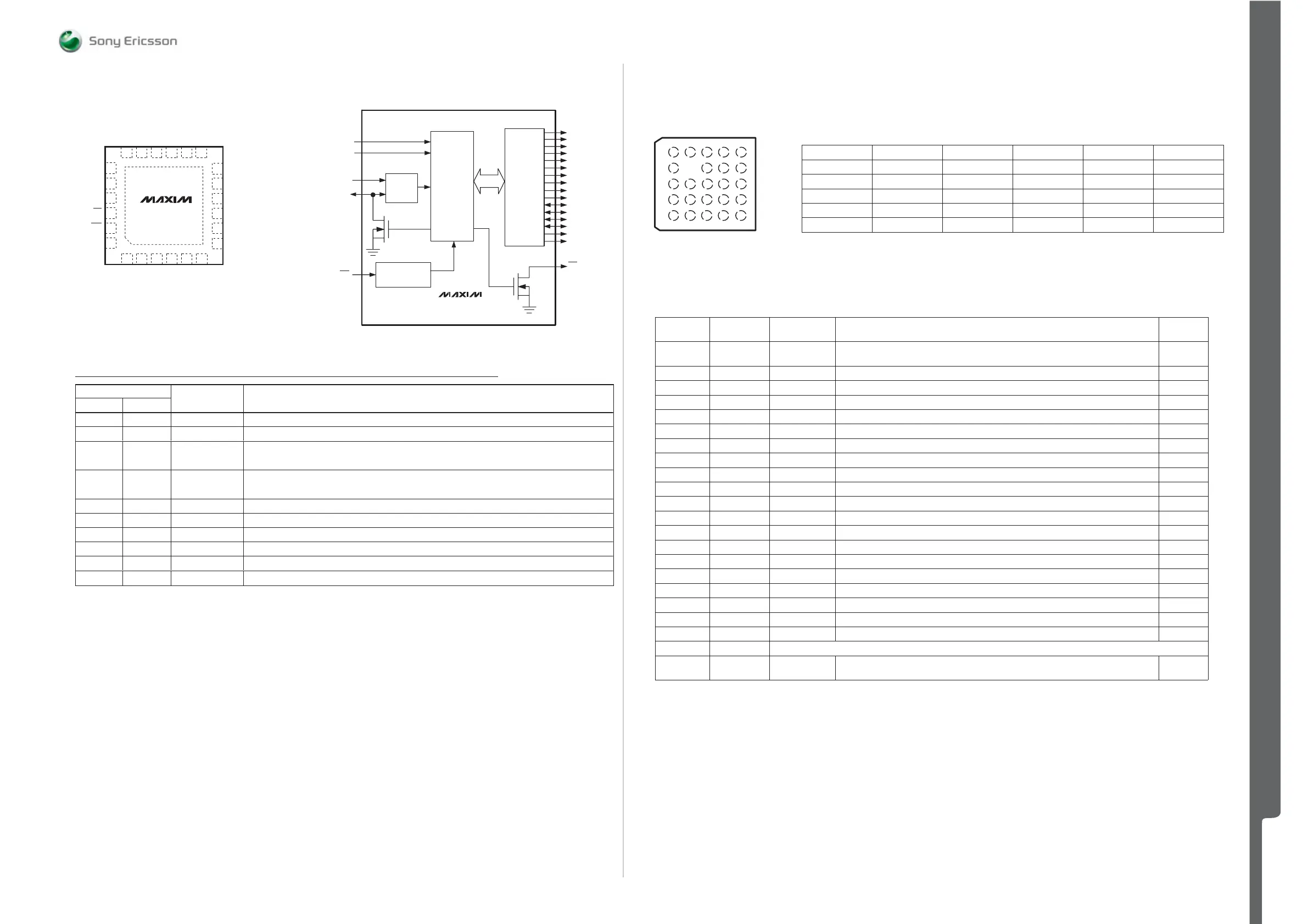
TERMINAL ASSIGNMENTS
12345
A DAT2A CMD-dir DAT0-dir RSV DAT2B
B DAT3A V
CCA
V
CCB
DAT3B
C CLKA RSV GND GND CLKB
D DAT0A CMDA RSV CMDB DAT0B
E DAT1A CLK-f DAT123-dir RSV DAT1B
PIN DESCRIPTION
GXY/ZXY GQS/ZQS
NAME FUNCTION TYPE
NO. NO.
Clock feedback to host for resynchronizing data. Used in OMAP processors.
A1 E2 CLK-f Output
Leave unconnected if not used.
A2 E1 DAT1A Data bit 2 connected to host. Referenced to V
CCA
. I/O
A3 C1 CLKA Clock signal connected to host. Referenced to V
CCA
. Input
A4 B1 DAT3A Data bit 4 connected to host. Referenced to V
CCA
. I/O
A5 B3 V
CCA
A-port supply voltage. V
CCA
powers all A-port I/Os and control inputs. Power
B1 D2 CMDA Command bit connected to host. Referenced to V
CCA
. I/O
B2 D1 DAT0A Data bit 1 connected to host. Referenced to V
CCA
. I/O
B3 C4 GND Ground
B4 A1 DAT2A Data bit 3 connected to host. Referenced to V
CCA
. I/O
B5 A2 CMD-dir Direction control for command bit (CMDA/CMDB) Input
C1 E3 DAT123-dir Direction control for DAT1A/B, DAT2A/B, and DAT3A/B Input
C2 D4 CMDB Command bit connected to memory card. Referenced to V
CCB
. I/O
C3 C3 GND Ground
C4 A5 DAT2B Data bit 3 connected to memory card. Referenced to V
CCB
I/O
C5 A3 DAT0-dir Direction control for DAT0A/DAT0B Input
D1 E5 DAT1B Data bit 2 connected to memory card. Referenced to V
CCB
. I/O
D2 D5 DAT0B Data bit 1 connected to memory card. Referenced to V
CCB
. I/O
D3 C5 CLKB Clock signal connected to memory card. Referenced to V
CCB
.Output
D4 B5 DAT3B Data bit 4 connected to memory card. Referenced to V
CCB
. I/O
D5 B4 V
CCB
B-port supply voltage. V
CCB
powers all B-port I/Os. Power
NA B2 Depopulated ball
A4, C2, D3,
NA RSV Reserved (for possible future functionality). Leave unconnected.
E4
D2420 IC IF 3.5x3.5x0.8 Thin QFN 1200-1951 D2460 Leveltranslator RYT109932/3
SEMC Troubleshooting Manual
77 (101)