K850
1203-2528 rev. 1
APPENDIX Components N2400 - N2402 - N2500
APPENDIX
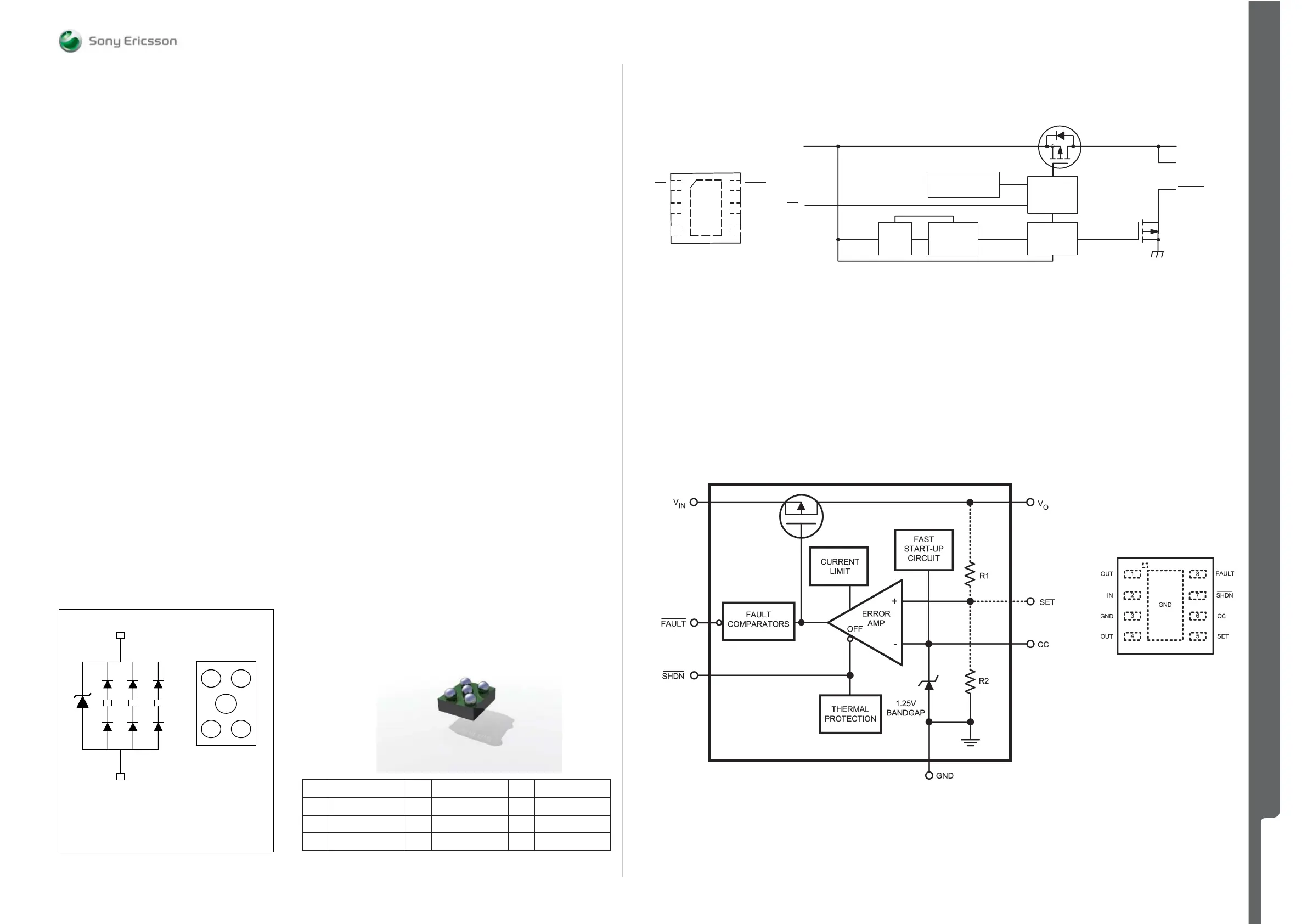
PIN DESCRIPTION PIN DESCRIPTION PIN DESCRIPTION
A1 D- B1 - C1 Vbus
A2 - B2 GND C2 ---
A3 D+ B3 C3 ID
Figure 1: IP4059CX5/LF
schematic pinning diagram
1
2
3
BAC
Bottom view
balls up
C1
B2
A1 A3 C3
PIN CONNECTIONS
IN
GND
FLAG
EN
OUT
OUT
1
2
3
6
5
4
UDFN
Functional Block Diagram
INPUT
LDO V
REF
UVLO
OVLO
Soft Start
OUTPUT
FLAGV
(2 out pins in
UDFN packa
Thermal Shutdown
EN
Functional Block Diagram
Top View
N2400 1-Bit Level Translator RYT109914/1 N2402 IC ESD Protection UDFN 6 2x2mm 1200-6309
N2401 IC ESD Protection 1200-0454
N2500 IC Voltage Regulator 8-pin LLP 1200-2552
SEMC Troubleshooting Manual
83 (101)