K850
1203-2528 rev. 1
APPENDIX Components N2205 - N2208
APPENDIX
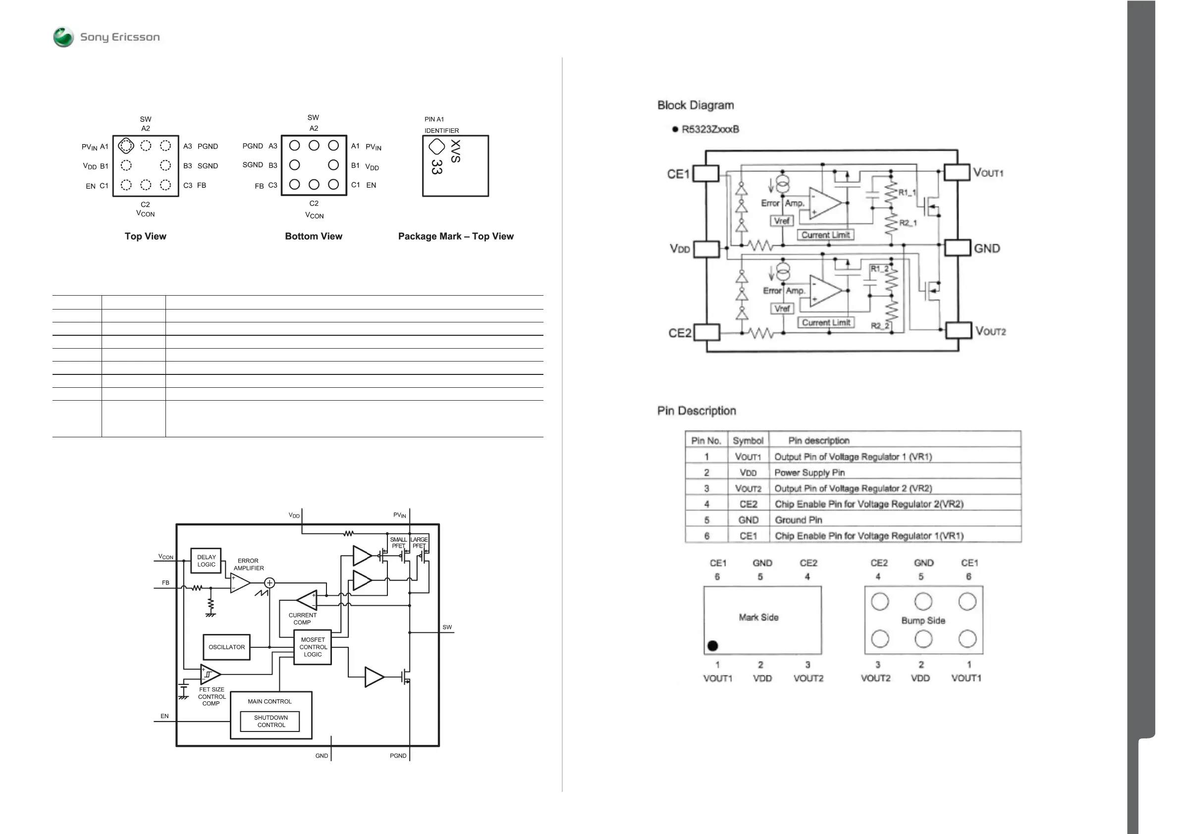
Connection Diagrams
Pin Descriptions
noitpircseDemaN#niP
A1 PV
IN
Power Supply Voltage Input to the internal PFET switch.
B1 V
DD
Analog Supply Input.
C1 EN Enable Input. Set this digital input high for normal operation. For shutdown, set this pin low.
C2 V
CON
Voltage Control Analog input. V
CON
controls V
OUT
in PWM mode.
C3 FB Feedback Analog Input. Connect to the output at the output lter capacitor.
B3 SGND Analog and Control Ground
A3 PGND Power Ground
A2 SW Switch node connection to the internal PFET switch and NFET synchronous rectier.
Connect to an inductor with a saturation current rating that exceeds the maximum Switch Peak
Current Limit specication of the LM3208.
Block Diagram
N2205 IC Voltage Regulator 1200-0107 N2208 IC Voltage Regulator RYT113997/4
SEMC Troubleshooting Manual
82 (101)
 Loading...