K850
1203-2528 rev. 1
APPENDIX Components N2525 - N3100 - N3101
APPENDIX
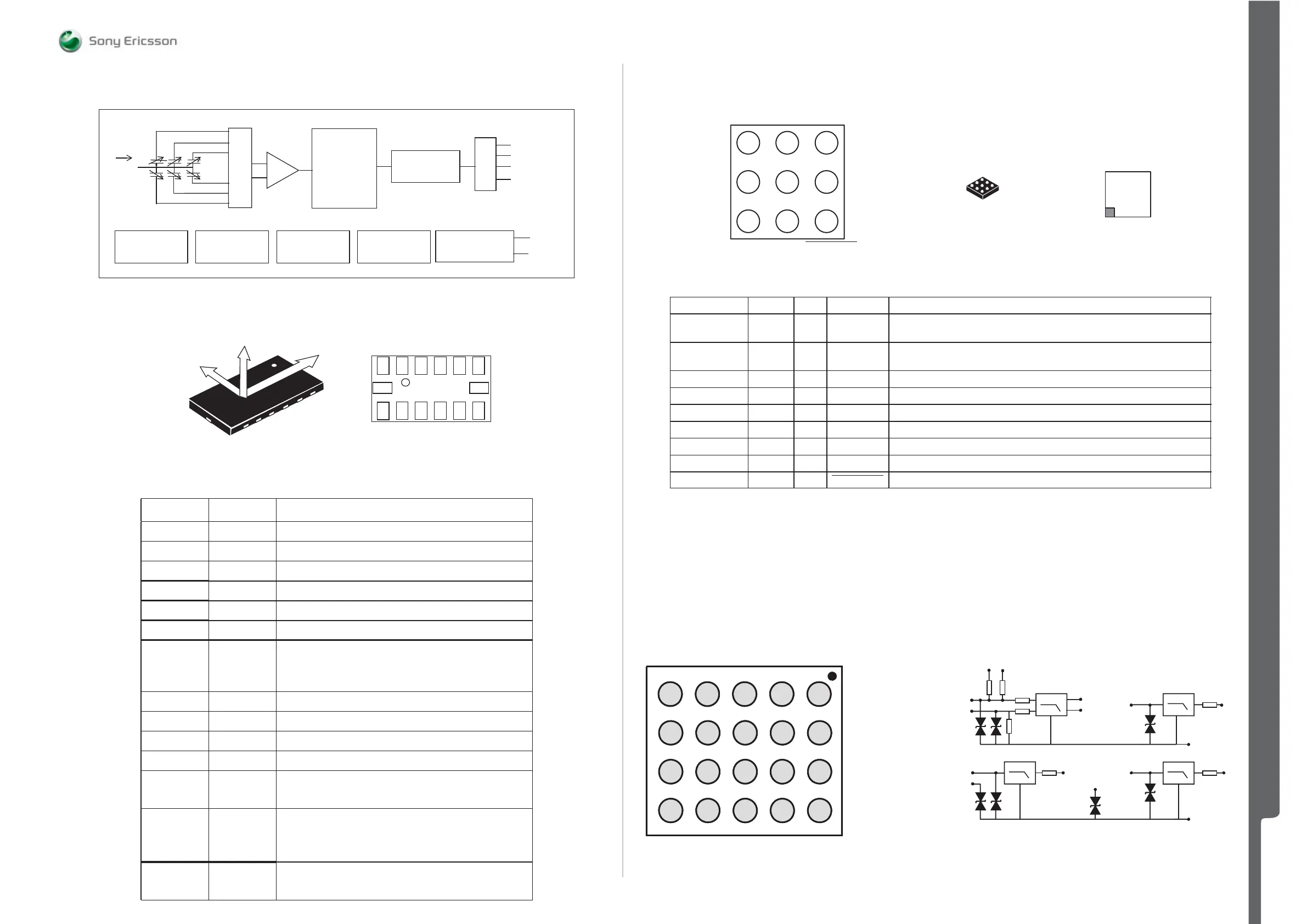
Block Diagram
CHARGE
AMPLIFIER
MUX
Y+
Z+
Y-
Z-
a
X+
X-
I
2
C
SPI
CS
SCL/SPC
SDA/SDO/SDI
SDO
CONTROL LOGIC
&
INTERRUPT GEN.
INT 1
CLOCK
TRIMMING
CIRCUITS
REFERENCESELF TEST
CONTROL LOGIC
A/D
CONVERTER
INT 2
Pin Connection
1
831
6
1
BOTTOM VIEW
13
8
6
TOP VIEW
X
Z
Y
Pin description
noitcnuFemaN#niP
1 Vdd_IO
Power supply for I/O pins
2GND
0V supply
3 Reserved
Connect to Vdd
4GND
0V supply
5GND
0V supply
6Vdd
Power supply
7CS
SPI enable
I
2
C/SPI mode selection (1: I
2
C mode; 0: SPI
enabled)
8INT 1
Inertial interrupt 1
9INT 2
Inertial interrupt 2
10 GND
0V supply
11 Reserved
Connect to Gnd
12 SDO
SPI Serial Data Output
I
2
C less significant bit of the device address
13
SDA
SDI
SDO
I
2
C Serial Data (SDA)
SPI Serial Data Input (SDI)
3-wire Interface Serial Data Output (SDO)
14
SCL
SPC
I
2
C Serial Clock (SCL)
SPI Serial Port Clock (SPC)
PIN CONNECTIONS
A3
B3
C3
A2
B2
C2
A1
B1
C1
INM OUTA INP
VM_P VM V
p
BYPASS OUTB SHUTDOWN
Microbump-9
(Top View)
Microbump-9
FC SUFFIX
CASE 499E
MARKING
DIAGRAMS
1
MAA
YYWW
A1
PIN DESCRIPTION
Microbump-9 Micro8 Type Symbol Description
A1 4 I INM Negative input of the first amplifier, receives the audio input signal. Connected
to the feedback resistor Rf and to the input resistor Rin.
A2 5 O OUTA Negative output of the NCP2890. Connected to the load and to the feedback
resistor Rf.
A3 3 I INP Positive input of the first amplifier, receives the common mode voltage.
B1 NA I VM_P Power Analog Ground.
B2 7 I VM Core Analog Ground.
B3 6 I V
p
Positive analog supply of the cell. Range: 2.5 V-5.5 V.
C1 2 I BYPASS Bypass capacitor pin which provides the common mode voltage (Vp/2).
C2 8 O OUTB Positive output of the NCP2890. Connected to the load.
C3 1 I SHUTDOWN The device enters in shutdown mode when a low level is applied on this pin.
Pin conguration (Bump side)
12345
A
B
C
D
VMIC SPRi
SPLi
MIC
Ni
MIC
Pi
INT
mice
Gnd
INT
mici
CCO VAD
Gnd
Gnd
Gnd
Gnd
Gnd
SPR
e
SPL
e
MIC
Ne
MIC
Pe
SPR
EF
1234152345
A
B
C
D
A
B
C
D
VMIC SPRi
SPLi
MIC
Ni
MIC
Pi
INT
mice
Gnd
INT
mici
CCO VAD
Gnd
Gnd
Gnd
Gnd
Gnd
SPR
e
SPL
e
MIC
Ne
MIC
Pe
SPR
EF
Electrical diagram
SPRi
SPLi
MICPe
GND
SPRe
SPREF
MICPi
MICNi
CCO/VMICVAD
MICNe
INTmici
SPLe
GND
CCO/VMIC
INTmice
R1
R7
R8R6
R4
R5
R3
R2
SPRi
SPLi
MICPe
GND
SPRe
SPREF
MICPi
MICNi
CCO/VMICVAD
MICNe
INTmici
SPLe
GND
CCO/VMIC
INTmice
R1
R7
R8R6
R4
R5
R3
R2
N2525 ASIC 3-axis Accelerometer 1200-1223 N3100 OPAMP 1W Pb-Free RYT101947/2
N3101 ASIC Tjatte 3 CSP20 ROP1013074/1
SEMC Troubleshooting Manual
84 (101)
 Loading...