33
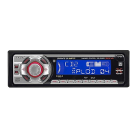
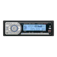
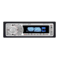
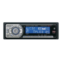
CDX-F5510/F5510X/F5550EE
CDX-F5510/F5510X/F5550EE
• NOTE FOR PRINTED WIRING BOARDS AND SCHEMATIC DIAGRAMS • WAVEFORMS
— MAIN BOARD —
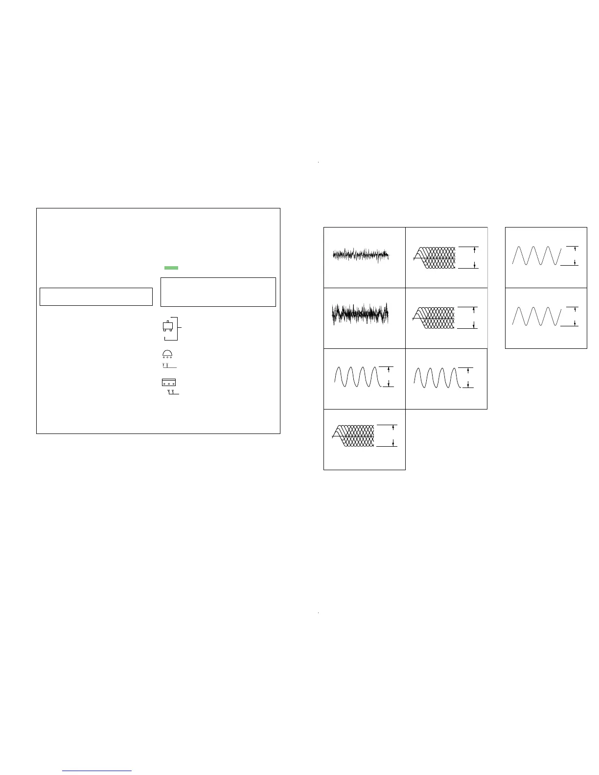
1
IC2 4 (FEI)
Approx.
1Vp-p
0 V
0.6 Vp-p
16.9344 MHz
Approx. 100 mVp-p
50 mV/DIV, 5 msec/DIV
0.5 V/DIV, 0.5
µ
sec/DIV
2
IC2 6 (TEI)
200 mV/DIV, 5 msec/DIV
6
IC2 oh (FPI2),
0.5 V/DIV, 0.5
µ
sec/DIV
Approx. 400 mVp-p
3
IC2 wd (XI)
0.2 V/DIV, 0.2
µ
sec/DIV
7
IC3 ia (X1)
0.5 V/DIV, 0.2
µ
sec/DIV
1.1 Vp-p
12 MHz
4
IC2 uj (RFI)
0.5 V/DIV, 0.5
µ
sec/DIV
5
IC2 of (FNI2),
og (FNI1)
1.5 Vp-p
oj (FPI1)
1.5 Vp-p
0 V
0.8 Vp-p
32.768 kHz
1 IC801 i; (XOA)
0.2 V/DIV, 20
µ
sec/DIV
1.2 Vp-p
18.432 MHz
2 IC801 id (X1)
0.5 V/DIV, 0.1
µ
sec/DIV
— SERVO BOARD —
(CD PLAY)
THIS NOTE IS COMMON FOR PRINTED WIRING
BOARDS AND SCHEMATIC DIAGRAMS.
(In addition to this, the necessary note is printed
in each block.)
For schematic diagrams.
Note:
• All capacitors are in µF unless otherwise noted. (p: pF)
50 WV or less are not indicated except for electrolytics
and tantalums.
• All resistors are in Ω and
1
/
4
W or less unless otherwise
specified.
•
f
: internal component.
• C : panel designation.
For printed wiring boards.
Note:
• X : parts extracted from the component side.
• Y : parts extracted from the conductor side.
•
a
: Through hole.
• : Pattern from the side which enables seeing.
(The other layers' patterns are not indicated.)
• A : B+ Line.
• B : B– Line.
• H : adjustment for repair.
•Voltages and waveforms are dc with respect to ground
under no-signal (detuned) conditions.
• CD mechanism section (1/2), (2/2)
no mark : CD PLAY
• Main section (1/3), (2/3), (3/3)
no mark : FM
(): AM
<>: CD PLAY
∗ : Impossible to measure
•Voltages are taken with a VOM (Input impedance 10 MΩ).
Voltage variations may be noted due to normal produc-
tion tolerances.
•Waveforms are taken with a oscilloscope.
Voltage variations may be noted due to normal produc-
tion tolerances.
• Circled numbers refer to waveforms.
• Signal path.
J : CD PLAY
F : FM
f : AM
L : BUS AUDIO
Caution:
Pattern face side: Parts on the pattern face side seen from the
(Side B) pattern face are indicated.
Parts face side: Parts on the parts face side seen from the
(Side A) parts face are indicated.
Q
C
These are omitted
EB
E
These are omitted
CB
C
These are omitted
BE
SECTION 1
DIAGRAMS
Note: The components identified by mark 0 or dotted line
with mark 0 are critical for safety.
Replace only with part number specified.
 Loading...