21 21
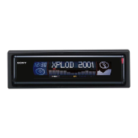
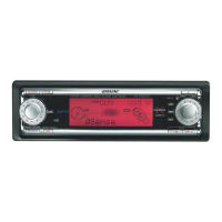
CDX-MP80
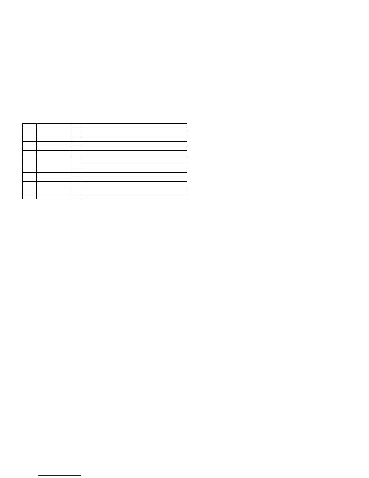
Pin No. Pin Name I/O Pin Description
98 UNI SI I Bus data input
99 VSS — Ground pin
100 VSS — Ground pin
101 UNI CKI I Bus clock signal input
102 NCO O Not used. (Open)
103 AVCC — Power supply pin (+5 V)
104 VREF — Reference voltage pin (+5 V)
105 – 111 NIL I Connecting to ground in this set.
112 SA IN I SA data input
113 AVSS — Ground pin
114 VSS — Ground pin
115 – 122 NCO O Not used. (Open)
123 MD0 (H) — Mode pin
124 MD1 (H) — Mode pin
125 MD2 (H) — Mode pin
126 – 128 NCO O Not used. (Open)
 Loading...