1515
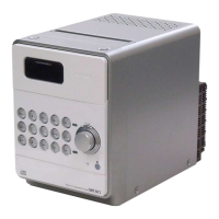
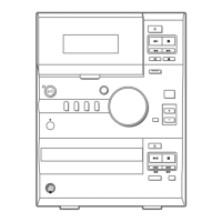
HCD-DF1
HCD-DF1
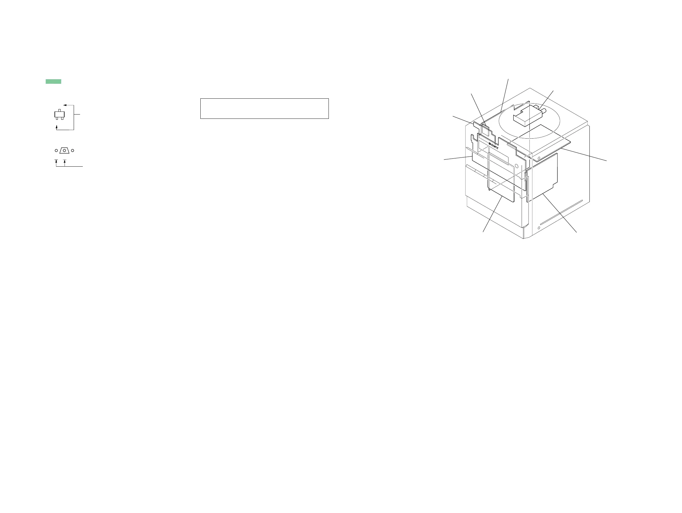
MICROPHONE board
PANEL board
DECK board
POWER SWITCH board
MAIN board
TUNER (FM/AM)
DVD board
POWER board
• Note for Printed Wiring Boards and Schematic Diagrams
C
B
These are omitted.
E
Q
Note on Schematic Diagram:
• All capacitors are in µF unless otherwise noted. (p: pF)
50 WV or less are not indicated except for electrolytics
and tantalums.
• All resistors are in Ω and
1
/
4
W or less unless otherwise
specified.
• C : panel designation.
• A : B+ Line.
• Voltages and waveforms are dc with respect to ground
under no-signal (detuned) conditions.
no mark : TUNER (FM/AM)
(): DVD PLAY
[]: TAPE PLAY
〈〈 〉〉 : REC
∗ : Impossible to measure
• Voltages are taken with a VOM (Input impedance 10 MΩ).
Voltage variations may be noted due to normal produc-
tion tolerances.
• Waveforms are taken with a oscilloscope.
Voltage variations may be noted due to normal produc-
tion tolerances.
• Circled numbers refer to waveforms.
• Signal path.
F : AUDIO
L : VIDEO
E : Y
a : CHROMA
r : COMPONENT VIDEO
J : DIGITAL OUT
f : TUNER (FM/AM)
d : TAPE PLAY
G : REC
N : MIC INPUT
• Abbreviation
AUS: Australian model
HK : Hong Kong model
KR : Korean model
RU : Russian model
SP : Singapore model
TW : Taiwan model
• Circuit Boards Location
Note on Printed Wiring Board:
• X : parts extracted from the component side.
• Y : parts extracted from the conductor side.
• x : parts mounted on the conductor side.
• : Pattern from the side which enables seeing.
(The other layers' patterns are not indicated.)
• Indication of transistor
Note: The components identified by mark 0 or dotted line
with mark 0 are critical for safety.
Replace only with part number specified.
B
These are omitted.
CE
Q
 Loading...