75
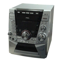
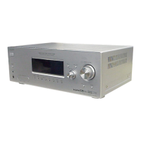
CX-BK1
• MAIN BOARD IC901 uPD703260YGF-S04-JBT-A (SYSTEM CONTROLLER)
Pin No. Pin Name I/O Description
1 RDS_SIG I
Tuning signal level input from the RDS decoder Used for the AEP, UK models
2 RDS_DATA I
Serial data input from the RDS decoder Used for the AEP, UK models
3 AVREF0 —
Reference voltage (+3.1V) input terminal
4 AVSS —
Ground terminal
5 MICS O
Chip select signal output to the MP3 decoder
6DOISerial data input from the tuner unit
7 AVREF1 — Power supply terminal (+3.1V)
8 STEREO I Stereo detection signal input from the tuner unit
9 TUNE I Tuner tuned status signal from the tuner unit
10 FLMD0 — Not used
11 VDD — Power supply terminal (+3.1V)
12 REGC —
Connected to the external capacitor
13 VSS — Ground terminal
14 X1 I
Main system clock input terminal (5MHz)
15 X2 O
Main system clock output terminal (5MHz)
16 RESET I
Reset signal input from the reset signal generator “L”: reset
17 XT1 I
Sub system clock input terminal (32.768kHz)
18 XT2 O
Sub system clock output terminal (32.768kHz)
19 MP3RST O System reset signal output to the MP3 decoder
20 RDS_CLK I
Clock signal input from the RDS decoder
Microphone detect signal input terminal
Used for the AEP, UK, Chilean, Peruvian models
21 SCOR I SCOR signal input from the digital signal processor
22 CAN'T_USE — Not used
23 RMC I Remote control signal input from the remote control receiver
24 USB_DATA I/O I2C data input/output with the USB interface IC
25 USB_CLK I/O I2C clock signal input/output to the USB interface IC
26 DECK_PLAYSW I PLAY switch signal input from the tape mechanism deck
27 DECK_ENDSW I END switch signal input from the tape mechanism deck
28 DECK_PACK I PACK switch signal input from the tape mechanism deck
29 DECK_FREC I Record protect detect switch signal input from the tape mechanism deck (front)
30 DECK_RREC I Record protect detect switch signal input from the tape mechanism deck (rear)
31 USB_ACK I Acknowledge signal input from the USB interface IC
32 USB_INT I Interrupt request signal input from the USB interface IC
33 USB_VBUS_ON O VBUS control signal output terminal
34 STBY O Standby LED control signal output terminal
35 EVSS — Ground terminal
36 EVDD — Power supply terminal (+3.1V)
37 MIACK I Acknowledge signal input from the MP3 decoder
38 MP3STB O Strobe signal output to the MP3 decoder
39 MUTE O Muting control signal output to power amplifier circuit
40 POWER O Main power control signal output terminal
41 POWER_DOWN I Power down detection signal input terminal
42 HEADPHONE I
Headphone detection signal input “L”: headphone on
43 SHIFT_CLK O Serial data transfer clock signal output to the shift register