EasyManua.ls Logo

Sony HCD-AZ2D Service Manual

Sony HCD-AZ2D
110 pages
To Next Page IconTo Next Page
Page #1 background imageLoading...
Page #1 background image
SERVICE MANUAL
DVD DECK RECEIVER
E Model
Australian Model
HCD-AZ2D/AZ5D
Ver. 1.0 2005.06
SPECIFICATIONS
9-879-718-01
2005F0579-1
© 2005.06
Sony Corporation
Audio Group
Published by Sony Engineering Corporation
HCD-AZ2D is the amplifier, disc player, tape
deck and tuner section in DHC-AZ2D.
HCD-AZ5D is the amplifier, disc player tape
deck and tuner section in DHC-AZ5D.
Amplifier section
HCD-AZ5D
The following measured at AC 120, 127, 220, 240 V,
50/60 Hz
DIN power output (rated): 75 + 75 watts
(4 ohms at 1 kHz, DIN)
Continuous RMS power output (reference)
Front speaker: 100 + 100 watts
(4 ohms at 1 kHz, 10%
THD)
Center speaker: 50 watts (8 ohms at 1 kHz,
10% THD)
Surround speaker: 50 + 50 watts
(8 ohms at 1 kHz, 10%
THD)
Subwoofer: 180 watts (2 ohms at
100 Hz, 10% THD)
HCD-AZ2D
The following measured at AC 120, 127, 220, 240 V,
50/60 Hz
DIN power output (rated): 75 + 75 watts
(4 ohms at 1 kHz, DIN)
Continuous RMS power output (reference)
100 + 100 watts
(4 ohms at 1 kHz, 10%
THD)
Inputs
VIDEO/SAT IN (audio) (phono jacks):
voltage 250/450 mV,
impedance 47 kilohms
MIC 1/MIC 2 (phone jacks):
sensitivity 1 mV,
impedance 10 kilohms
Outputs
VIDEO/SAT OUT (audio) (phono jacks):
voltage 250 mV,
impedance 1 kilohm
VIDEO OUT (phono jack):
max. output level
1 Vp-p, unbalanced, Sync
negative, load impedance
75 ohms
S VIDEO OUT (4-pin/mini-DIN jack):
Y: 1 Vp-p, unbalanced,
Sync negative,
C: 0.286 Vp-p, load
impedance 75 ohms
COMPONENT VIDEO OUT:
Y: 1 Vp-p, 75 ohms
P
B, PR: 0.7 Vp-p, 75 ohms
DVD DIGITAL OUT (DHC-AZ2D only)
(Square optical connector jack, rear panel)
Wavelength660 nm
PHONES (stereo mini jack):
accepts headphones of
8ohms or more
FRONT SPEAKER: Use only the supplied
speaker SS-AZ7D.
SURROUND SPEAKER (HCD-AZ5D only):
Use only the supplied
speaker SS-RS7D.
CENTER SPEAKER (HCD-AZ5D only):
Use only the supplied
speaker SS-CT7D.
SUBWOOFER (HCD-AZ5D only):
Use only the supplied
speaker SS-WG7D.
Disc player section
System Compact disc and digital
audio and video system
Laser Semiconductor laser
(DVD: λ =650 nm,
CD: λ =790 nm)
Emission duration:
continuous
Frequency response DVD (PCM 48 kHz):
2 Hz 22 kHz (±1 dB)
CD: 2 Hz 20 kHz (±1 dB)
Video color system format
Latin American model:
NTSC
Other models: NTSC, PAL
DVD
Model Name Using Similar Mechanism NEW
Section
DVD Mechanism Type CDM86-DVBU101
Optical Pick-up Block Name KHM-310CAB
Tape deck-A Model Name Using Similar Mechanism NEW
Section Tape Transport Mechanism Type CMAL5Z230
Tape deck-B Model Name Using Similar Mechanism NEW
Section Tape Transport Mechanism Type CMAL1Z254A
This system incorporates Dolby
1)
Digital, Dolby Pro
Logic (II) adaptive matrix surround decoder, and
DTS
2)
Digital Surround System.
1)
Manufactured under license from Dolby
Laboratories.
“Dolby”, “Pro Logic”, and the double-D symbol are
trademarks of Dolby Laboratories.
2)
Manufactured under license from Digital Theater
Systems, Inc. “DTS” and “DTS Digital Surround”
are registered trademarks of Digital Theater
Systems, Inc.
– Continued on next page –
Photo: HCD-AZ5D
w
w
w
.
x
i
a
o
y
u
1
6
3
.
c
o
m
Q
Q
3
7
6
3
1
5
1
5
0
9
9
2
8
9
4
2
9
8
T
E
L
1
3
9
4
2
2
9
6
5
1
3
9
9
2
8
9
4
2
9
8
0
5
1
5
1
3
6
7
3
Q
Q
TEL 13942296513 QQ 376315150 892498299
http://www.xiaoyu163.com

Table of Contents

Question and Answer IconNeed help?

Do you have a question about the Sony HCD-AZ2D and is the answer not in the manual?

Sony HCD-AZ2D Specifications

General IconGeneral
TypeReceiver
ModelHCD-AZ2D
Tuner BandsFM/AM
CD PlayerYes
USB Playback/PortYes
BluetoothNo
Speaker load impedance6 ohms
Digital inputsNo
Remote ControlYes
OutputHeadphone
Audio Channels2

Summary

SPECIFICATIONS

Amplifier section

Details amplifier performance specifications.

Outputs

Lists output specifications for various signal types.

Disc player section

Specifications for the disc playback mechanism.

SELF DIAGNOSIS FUNCTION

First 3 characters of the service number

Identifies service codes and their causes/corrections.

Tuner section

SERVICING NOTES

DISASSEMBLY

3-1. DISASSEMBLY FLOW

Visual flowchart of the disassembly process.

3-8. DVD MECHANISM DECK (CDM86-DVBU101)

Procedure for removing the DVD mechanism deck.

3-9. OPTICAL PICK-UP BLOCK (KHM-310CAB)

Procedure for removing the optical pick-up block.

TEST MODE

COLD RESET

Procedure to reset the system to initial conditions.

PANEL TEST MODE

Checks display, model, software version, and keys.

MEMORY CLEAR MODE

Clears microprocessor data to initial conditions.

MECHANICAL ADJUSTMENTS

ELECTRICAL ADJUSTMENTS

DECK SECTION

Electrical adjustments for the deck section.

RECORD/PLAYBACK HEAD AZIMUTH ADJUSTMENT

Procedure for adjusting head azimuth for both decks.

DIAGRAMS

7-1. BLOCK DIAGRAM – RF SERVO/VIDEO SECTION –

Block diagram of RF servo and video circuits.

7-3. BLOCK DIAGRAM – AUDIO SECTION –

Block diagram of the audio signal path.

7-4. BLOCK DIAGRAM – AMP SECTION –

Block diagram of the amplifier section.

7-5. BLOCK DIAGRAM – PANEL/POWER SUPPLY SECTION –

Block diagram of panel and power supply circuits.

7-6. PRINTED WIRING BOARD – DMB10 BOARD (SIDE A) –

Component layout for DMB10 board, side A.

7-7. PRINTED WIRING BOARD – DMB10 BOARD (SIDE B) –

Component layout for DMB10 board, side B.

7-8. SCHEMATIC DIAGRAM – DMB10 BOARD (1/4) –

Schematic of DMB10 board, part 1 of 4.

7-9. SCHEMATIC DIAGRAM – DMB10 BOARD (2/4) –

Schematic of DMB10 board, part 2 of 4.

7-10. SCHEMATIC DIAGRAM – DMB10 BOARD (3/4) –

Schematic of DMB10 board, part 3 of 4.

7-11. SCHEMATIC DIAGRAM – DMB10 BOARD (4/4) –

Schematic of DMB10 board, part 4 of 4.

7-14. PRINTED WIRING BOARD – MAIN BOARD –

Component layout for the main board.

7-15. SCHEMATIC DIAGRAM – Main Board (1/4) –

Schematic of main board, part 1 of 4.

7-16. SCHEMATIC DIAGRAM – Main Board (2/4) –

Schematic of main board, part 2 of 4.

7-17. SCHEMATIC DIAGRAM – Main Board (3/4) –

Schematic of main board, part 3 of 4.

7-18. SCHEMATIC DIAGRAM – Main Board (4/4) –

Schematic of main board, part 4 of 4.

7-19. PRINTED WIRING BOARD – S-MASTER BOARD (Component Side) –

Component layout for S-MASTER board, component side.

7-20. PRINTED WIRING BOARD – S-MASTER BOARD (Conductor Side) –

Component layout for S-MASTER board, conductor side.

7-21. SCHEMATIC DIAGRAM – S-MASTER BOARD (1/4) –

Schematic of S-MASTER board, part 1 of 4.

7-22. SCHEMATIC DIAGRAM – S-MASTER BOARD (2/4) –

Schematic of S-MASTER board, part 2 of 4.
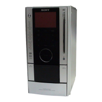
EXPLODED VIEWS

ELECTRICAL PARTS LIST

Related product manuals