68
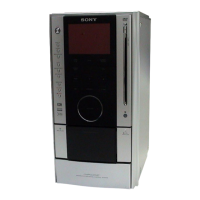
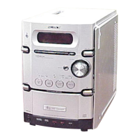
HCD-AZ2D/AZ5D
Pin No. Pin Name I/O Description
53 to 61
IOA2 to IOA8,
OAddress signal output to the flash ROM
IOA18, IOA19
62 DVSS – Ground terminal
63 APLLCAP – Connection terminal for an external capacitor
64 APLLVSS – Ground terminal
65 VDD3 – Power supply terminal (+3.3V)
66 IOWR O Write enable signal output to the flash ROM
67 to 72 IOA16 to IOA11 O Address signal output to the flash ROM
73 DVDD3 – Power supply terminal (+3.3V)
74 to 76 IOA10, IOA9,IOA20 O Address signal output to the flash ROM
77 IOCS O Chip select signal output to the flash ROM
78 IOA1 O Address signal output to the flash ROM
79 IOOE O Output enable signal output to the flash ROM
80 DVDD3 – Power supply terminal (+3.3V)
81 to 84 AD0 to AD3 I/O Data/address signal input/output terminal with the flash ROM
85 DVSS – Ground terminal
86 to 88 AD4 to AD6 I/O Data/address signal input/output terminal with the flash ROM
89 IOA21 O Address signal output to the flash ROM
90 ALE O Address latch enable signal output terminal Not used
91 AD7 I/O Data/address signal input/output terminal with the flash ROM
92, 93 IOA17, IOA0 O Address signal output to the flash ROM
94 DVSS – Ground terminal
95 UWR O Write enable signal output terminal Not used
96 URD O Data read enable signal output terminal Not used
97 DVDD18 – Power supply terminal (+1.8V)
98 IFSDO O Serial data output to the system controller
99 IFCK I Serial data transfer clock signal input from the system controller
100 XIFCS I Chip select signal input from the system controller
101 IFSDI I Serial data input from the system controller
102 SCL O Serial data transfer clock signal output to the EEPROM and D/A converter
103 SDA I/O Two-way data bus with the EEPROM and D/A converter
104 TRG-SW I Trigger detection switch input terminal
105 IFBSY I Busy signal input from the system controller
106 RXD I
Receive data input terminal for UART communication when data writing to
flash memory
107 TXD O
Transmit data output terminal for UART communication when data writing to
flash memory
108 DVDD3 – Power supply terminal (+3.3V)
109 ICE I ICE mode enable signal input terminal Not used
110 PRST I Reset signal input from the system controller “L”: reset
111 IR I IR control signal input terminal Not used
112 INT0 O Interrupt request signal output terminal Not used
113 DQM0 O Data mask signal output to the SD-RAM
114 MREQ O Muting request signal output to the system controller
115 RD7 I/O Two-way data bus with the SD-RAM
116 DVSS – Ground terminal
117, 118 RD6, RD5 I/O Two-way data bus with the SD-RAM
119 DVSS – Ground terminal
120, 121 RD4, RD3 I/O Two-way data bus with the SD-RAM
122 DVDD18 – Power supply terminal (+1.8V)
w
w
w
.
x
i
a
o
y
u
1
6
3
.
c
o
m
Q
Q
3
7
6
3
1
5
1
5
0
9
9
2
8
9
4
2
9
8
T
E
L
1
3
9
4
2
2
9
6
5
1
3
9
9
2
8
9
4
2
9
8
0
5
1
5
1
3
6
7
3
Q
Q
TEL 13942296513 QQ 376315150 892498299
TEL 13942296513 QQ 376315150 892498299
http://www.xiaoyu163.com
http://www.xiaoyu163.com