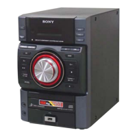
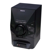
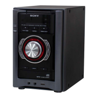
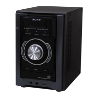
HCD-EC69/EC79/EC99
40
Pin No. Pin Name I/O Description
56 IPF O Not used
57 SFSY/LOCK O Not used
58 ZDET O Zero detection signal output terminal Not used
59 GPIN I Not used
60 MS I Microcomputer interface mode selection signal input terminal Fixed at “H” in this set
61 DOUT (PO6) O Digital audio data output terminal Not used
62 AOUT1 (PO7) O Audio data output terminal Not used
63 BCK (PO8) O Bit clock signal output terminal Not used
64 LRCK (PO9) O L/R sampling clock signal output terminal Not used
65 AIN (PI4) I Digital audio data input terminal Not used
66 BCKi (PI5) I Bit clock signal input terminal Not used
67 LRCKi (PI6) I L/R sampling clock signal input terminal Not used
68 VDD1 - Power supply terminal (+1.5V)
69 VSS1 - Ground terminal
70 AWRC - Not used
71 PVDD3 - Power supply terminal (+3.3V)
72 PDo O Phase error margin signal between EFM signal and PLCK signal output terminal
73 TMAXS O TMAX detection signal output terminal Not used
74 TMAX O TMAX detection signal output terminal
75 LPFN I Inverted signal input from the operation amplifi er for PLL loop fi lter
76 LPFo O Signal output from the operation amplifi er for PLL loop fi lter
77 PVREF I Reference voltage (+1.65V) input terminal
78 VCOF O VCO fi lter output terminal
79 PVSS3 - Ground terminal
80 SLCo O EFM slice level output terminal
81 RFi I RF signal input terminal
82 RFRPi I RF ripple signal input terminal
83 RFEQo O EFM slice level output terminal
84 VRo O Reference voltage (+1.65V) output terminal
85 RESiN O External resistor connection terminal
86 VMDiR O Reference voltage (+1.65V) output terminal for automatic power control circuit
87 TESTR O Low-pass fi lter terminal for RFEQO offset correction
88 AGCi I RF signal amplitude adjustment amplifi cation input terminal
89 RFo O RF signal generation amplifi cation output terminal
90 RVDD3 - Power supply terminal (+3.3V)
91 LDo O
Laser diode on/off control signal output to the automatic power control circuit
“H”: laser diode on
92 MDi I Light amount monitor input from the laser diode of optical pick-up block
93 RVSS3 - Ground terminal
94 FNi2 (C) I Main beam (C) input from the optical pick-up block
95 FNi1 (A) I Main beam (A) input from the optical pick-up block
96 FPi2 (D) I Main beam (D) input from the optical pick-up block
97 FPi1 (B) I Main beam (B) input from the optical pick-up block
98 TPi (F) I Sub beam (F) input from the optical pick-up block
99 TNPC O External capacitor connection terminal
100 TNi (E) I Sub beam (E) input from the optical pick-up block