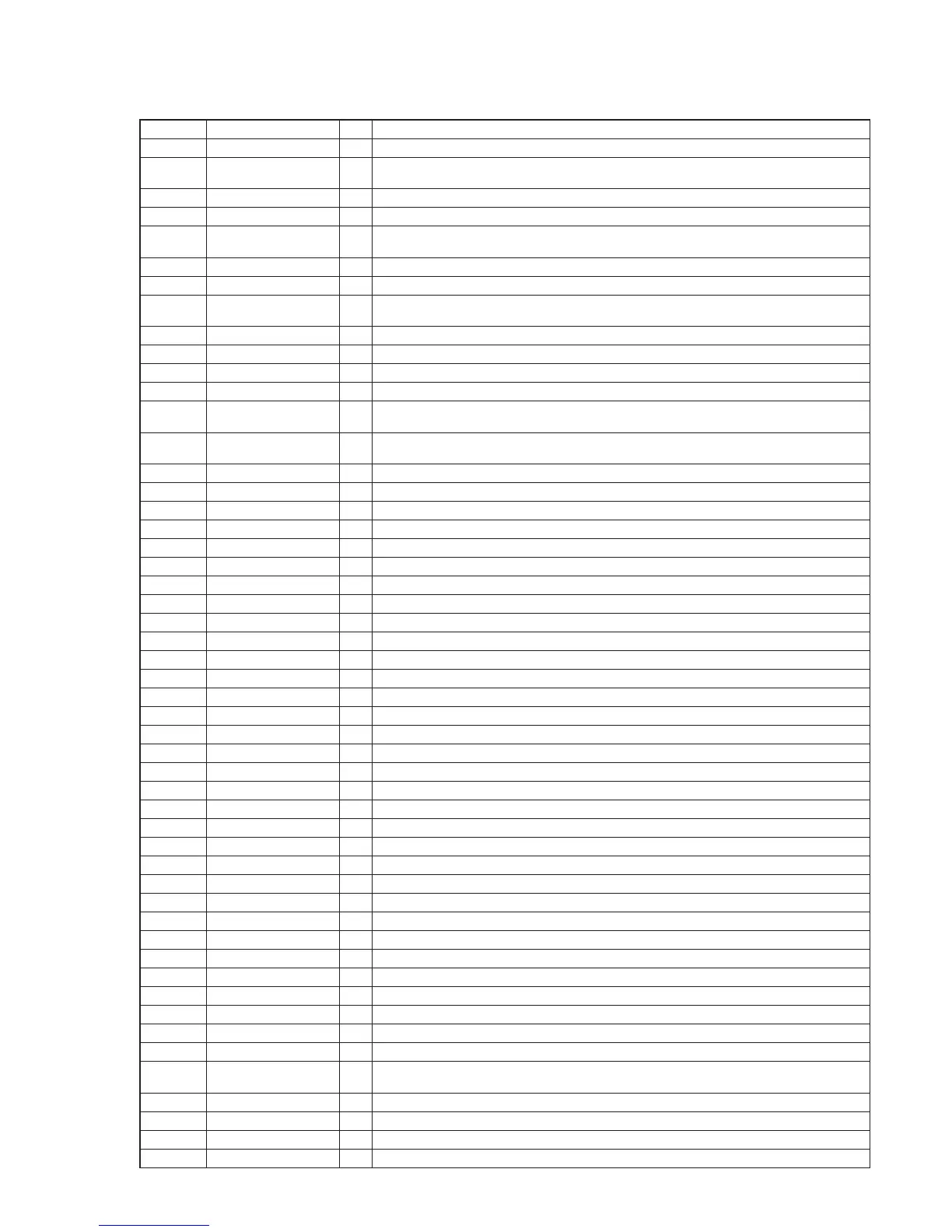
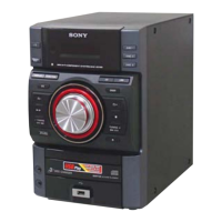
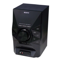
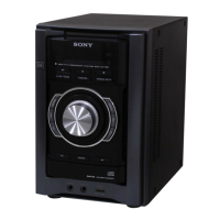
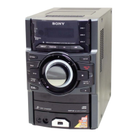
HCD-EC69/EC79/EC99
43
PANEL BOARD IC301 MB90F830PF-GE1 (SYSTEM CONTROLLER)
Pin No. Pin Name I/O Descriptio
1 SEG32 O Segment drive signal output to the liquid crystal display
2
O-SP-RELAY-ON/
TC ON/SW ON
O
Relay drive signal output terminal (for speaker), and subwoofer function on/off control signal
output terminal (EC99)
3 O-POWER O Main power on/off control signal output terminal “H”: main power on
4 O-CD-ON/5V ON O CD and VBUS power on/off control signal output terminal “H”: CD and VBUS power on
5 to 7
I-3CD-SW3 to
I-3CD-SW1
I Detection switch input from the CD mechanism deck
8 O-3CD-M1+ O Motor drive signal output to the CD mechanism deck
9 I-RMC I Remote control signal input from the remote control receiver
10 to 12
O-3CD-M1-, O-3CD-
M2+, O-3CD-M2-
O Motor drive signal output to the CD mechanism deck
13 X0A I Sub system clock input terminal (32.768 kHz)
14 X1A O Sub system clock output terminal (32.768 kHz)
15 VCC - Power supply terminal (+3.3V)
16 VSS - Ground terminal
17 to 20
I/O-CD-BUS0 to
I/O-CD-BUS3
O Serial data output to the CD-MP3 processor
21, 22
I-3CD-CHACK,
I-3CD-STOCK
I Detection switch input from the CD mechanism deck
23 O-DR-MUTE O Motor drive on/off control signal output to the motor/coil driver
24 I-REQ I Request signal input from the CD-MP3 processor
25 O-CD-BUCK O Serial data transfer clock signal output to the CD-MP3 processor
26 O-CD-CCE O Chip enable signal output to the CD-MP3 processor
27 O-CD-RST O System reset signal output to the CD-MP3 processor “L”: reset
28 O-LED O LED drive signal output terminal for standby indicator
29 I-USB-BUSY I Busy signal input from the USB controller
30 O-TP_REC_MUTE O Not used
31 O-USB-RST O System reset signal output to the USB controller “L”: reset
32 AVCC - Power supply terminal (+3.3V)
33 O-AUDIO-DATA O Serial data output to the electrical volume
34 O-AUDIO-CLK O Serial data transfer clock signal output to the electrical volume
35 AVSS - Ground terminal
36 I-P-MONI I Power monitor signal input terminal
37, 38 I-KEY1, I-KEY2 I Front panel key input terminal (A/D input)
39 I-TU-ANSD I Auto gain control signal input terminal
40 I-5V/9V-DET I Power supply voltage detection signal input terminal
41 I-KEY-WAKE-UP/VOL I Front panel key input terminal (A/D input)
42 I-HOLD I Hold signal input terminal
43 O-CD-SBSY I Subcode block sync signal input from the CD-MP3 processor
44 GND - Ground terminal
45 I-3CD-CLOSE/OPEN I Detection switch input from the CD mechanism deck
46 I-MODEL I Model setting terminal
47 I-SUFFIX/TP-STATE I Suffi x setting terminal
48 I-TU-DO I Serial data input from the AM/FM DET
49 I/O-I2C-DATA-USB I/O Serial data input/output with the USB controller
50 I/O-I2C-CLK-USB O Serial data transfer clock signal output to the USB controller
51 to 53 MD2 to MD0 - Not used
54 I-RST I Reset signal input from the reset switch “L”: reset
55 O-TU-CE O Chip enable signal output to the AM/FM DET
56 O-TU-DI O Serial data output to the AM/FM DET
57 O-TU-CLK O Serial data transfer clock signal output to the AM/FM DET
58 VLCD -
Terminal for doubler circuit capacitor connection to develop liquid crystal display drive volt-
age
59 to 62 COM0 to COM3 O Common drive signal output to the liquid crystal display
63, 64 SEG0, SEG1 O Segment drive signal output to the liquid crystal display
65 VCC - Power supply terminal (+3.3V)
66 VSS - Ground terminal