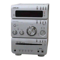
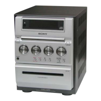
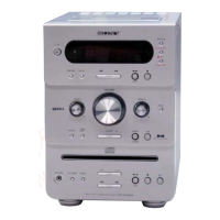
HCD-GPZ6/GPZ7
2323
HCD-GPZ6/GPZ7
• Note for Printed Wiring Boards and Schematic Diagrams
Note on Printed Wiring Board:
• X : parts extracted from the component side.
• Y : parts extracted from the conductor side.
• W : indicates side identified with part number.
•
f
: internal component.
• : Pattern from the side which enables seeing.
(The other layers' patterns are not indicated.)
Caution:
Pattern face side: Parts on the pattern face side seen from
(Conductor Side) the pattern face are indicated.
Parts face side: Parts on the parts face side seen from
(Component Side) the parts face are indicated.
• Indication of transistor.
C
B
These are omitted.
E
Q
B
These are omitted.
CE
Q
Note on Schematic Diagram:
• All capacitors are in µF unless otherwise noted. (p: pF)
50 WV or less are not indicated except for electrolytics
and tantalums.
• All resistors are in Ω and
1
/
4
W or less unless otherwise
specified.
• f : internal component.
• 2 : nonflammable resistor.
• 5 : fusible resistor.
• C : panel designation.
• A : B+ Line.
• Voltages and waveforms are dc with respect to ground
under no-signal (detuned) conditions.
– BD Board –
no mark : CD PLAY
– Other Section –
no mark : TUNER
(): CD PLAY
[]: TAPE PLAY
〈〈 〉〉 : TAPE REC
• Voltages are taken with a VOM (Input impedance 10 MΩ).
Voltage variations may be noted due to normal produc-
tion tolerances.
• Waveforms are taken with a oscilloscope.
Voltage variations may be noted due to normal produc-
tion tolerances.
• Circled numbers refer to waveforms.
• Signal path.
F : TUNER
E : TAPE PLAY
a : TAPE REC
J : CD PLAY (ANALOG)
c : CD PLAY (DIGITAL)
L : AUX IN
• Abbreviation
AR : Argentina model
AUS: Australian model
E51 : Chilean and Peruvian models
EE : East European model
KR : Korean model
MX : Mexican model
RU : Russian model
SP : Singapore model
Note: The components identified by mark 0 or dotted line
with mark 0 are critical for safety.
Replace only with part number specified.
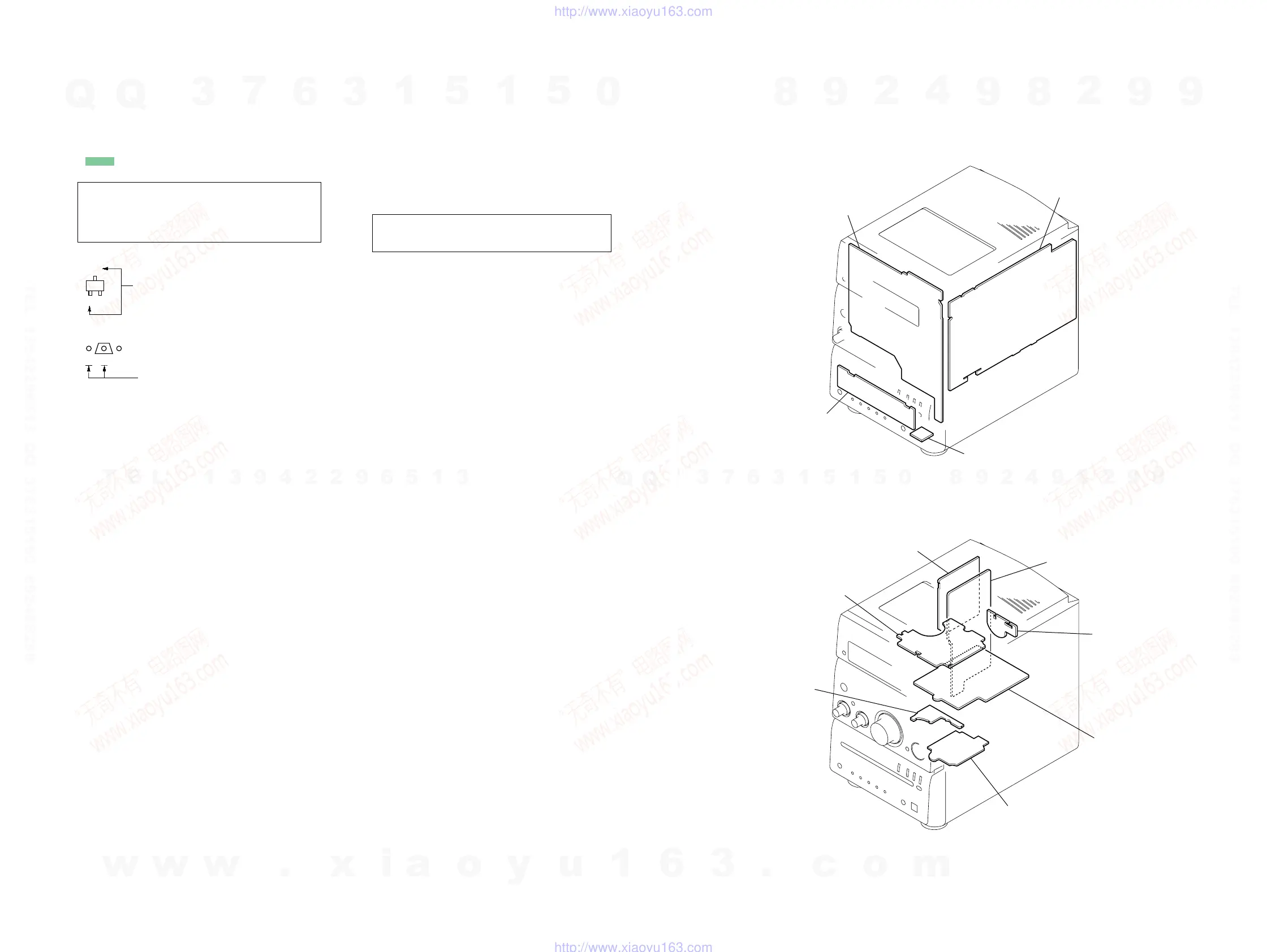
• Circuit Boards Location
MAIN board
PANEL (1) board
PANEL (2) board
OPTICAL board
BD board
AMP board
THERMISTOR board
POWER board
SUB PT board
AU-TC board
DRIVER board
Ver. 1.1
w
w
w
.
x
i
a
o
y
u
1
6
3
.
c
o
m
Q
Q
3
7
6
3
1
5
1
5
0
9
9
2
8
9
4
2
9
8
T
E
L
1
3
9
4
2
2
9
6
5
1
3
9
9
2
8
9
4
2
9
8
0
5
1
5
1
3
6
7
3
Q
Q
TEL 13942296513 QQ 376315150 892498299
TEL 13942296513 QQ 376315150 892498299
http://www.xiaoyu163.com
http://www.xiaoyu163.com