49
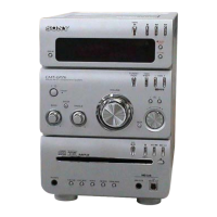
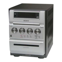
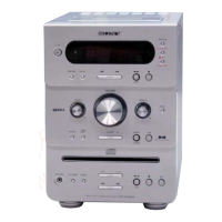
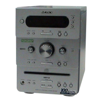
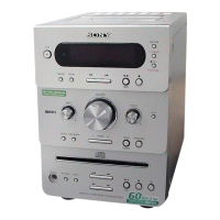
HCD-GPZ6/GPZ7
MAIN BOARD IC306 M30624MGP-A38FPU0 (SYSTEM CONTROLLER)
Pin No. Pin Name I/O Description
1, 2
CD DISCSEN2,
CD DISC SEN1
-
Not used
3 STBY LED O LED drive signal output terminal "H": standby
4
SIRCS IN/WAKE
I
Remote control signal input terminal
5
MP3 DATA OUT
O
MP3 serial data output to the CD DSP
6 MP3 DATA IN
I
MP3 serial data input from the CD DSP
7 MP3 CLK
O
MP3 serial data transfer clock signal output to the CD DSP
8
BYTE I
External data bus line byte selection signal input fixed at "L"
9
CNVSS -
Processor mode switch terminal (for test)
10 XCIN
I
Sub system clock input terminal (32.768 kHz)
11 XCOUT
O
Sub system clock output terminal (32.768 kHz)
12 RESET
I
System reset signal input terminal "L": reset
For several hundreds msec. after the power supply rises, "L" is input, then it changes to "H"
13 XOUT
O
Main system clock output terminal (16 MHz)
14 VSS
-
Ground terminal
15 XIN
I
Main system clock input terminal (16 MHz)
16 VCC
-
Power supply terminal (+3.3V)
17
NMI I Non-maskable interrupt input terminal Not used
18
RDS-CLK I
Serial data transfer clock signal input from the RDS decoder on the tuner unit
Used for AEP, UK, East European, Russian models
19
CD SCOR I
Sub-code sync (S0+S1) detection signal input from the CD DSP
20 AC-CUT
I
AC detection signal input terminal "L": AC off
21
RDS DATA
I
Serial data input from the RDS decoder on the tuner unit
Used for AEP, UK, East European, Russian models
22 CD XRST O Reset signal output to the CD DSP "L": reset
23 CD XLT
O
CD serial data latch pulse output to the CD DSP
24 MP3 ACK
O
MP3 acknowledge signal output to the CD DSP
25 MP3 XLAT
O
MP3 serial data latch pulse output to the CD DSP
26 MP3 REQ
O
MP3 chip select signal output to the CD DSP
27
MP3 IREQ O
MP3 data request signal output to the CD DSP
28
MP3 STB
O MP3 standby on/off control signal output terminal "L": standby
29
IIC CLK
O IIC data reading clock signal input or transfer clock signal output terminal Not used
30
IIC DATA I/O
IIC two-way data bus terminal Not used
31
SDA
O Serial data output terminal Not used
32
SCL
O Serial data transfer clock signal output terminal Not used
33 XTCN O
Oscillation circuit on/off switch control signal output to the CD DSP
"H": self-oscillation, "L": oscillation stop
34 CD BD POWER O CD power on/off control signal output terminal "H": power on
35 CD DATA
O
CD serial data output to the CD DSP
36 CD SENS I SENS signal output to the CD DSP
37 CD CLK
O
CD serial data transfer clock signal output to the CD DSP
38
CD AMUTE O
CD muting on/off selection signal output terminal "H": muting
39 FL DATA
O
Serial data output to the FL driver
40
ELV E3/TRE A I
Jog dial pulse input from the rotary encoder for the treble (A phase input)
41
ELV E2/TRE B I
Jog dial pulse input from the rotary encoder for the treble (B phase input)
42
ELV E1/BASS A I
Jog dial pulse input from the rotary encoder for the bass (A phase input)
43
ELV E0/BASS B I
Jog dial pulse input from the rotary encoder for the bass (B phase input)
Ver. 1.1
w
w
w
.
x
i
a
o
y
u
1
6
3
.
c
o
m
Q
Q
3
7
6
3
1
5
1
5
0
9
9
2
8
9
4
2
9
8
T
E
L
1
3
9
4
2
2
9
6
5
1
3
9
9
2
8
9
4
2
9
8
0
5
1
5
1
3
6
7
3
Q
Q
TEL 13942296513 QQ 376315150 892498299
TEL 13942296513 QQ 376315150 892498299
http://www.xiaoyu163.com
http://www.xiaoyu163.com