62
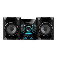
HCD-GX470/GX570
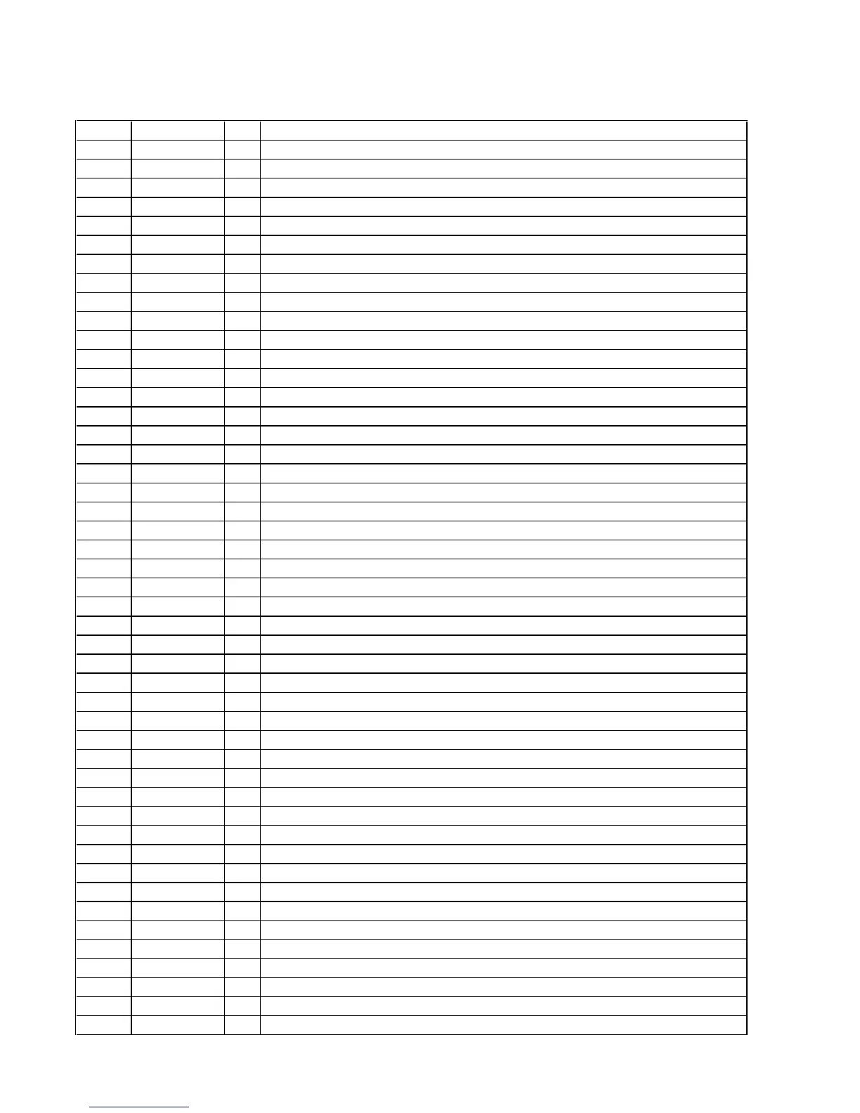
XM BOARD IC001 F2602E-01-TR (XM RECEIVER) (GX570)
Pin No.
Pin Name I/O Description
1
LSDP_TXRX - Not used
2
VSS - Ground terminal
3
SC_XT_OUT O Serial data output to the system controller
4
VDD - Power supply terminal (+3.3V)
5
SC_RX_IN I Serial data input from the system controller
6
VSS - Ground terminal
7
CDM_SEL I Command mode select signal input from the system controller
8
VDD - Power supply terminal (+3.3V)
9
ERR_IRQ# O Interrupt request signal output to the system controller
10
VSS - Ground terminal
11
RST# I Reset signal input from the system controller
12
SLAVE_SET I
Master/slave mode setting terminal "L": Master mode, "H": Slave mode Fixed at "L" in this set
13
COMM_RX_DIG - Not used
14
COMM_TX_DIG - Not used
15
COMM_TX_EN - Not used
16
VSS - Ground terminal
17
VDD - Power supply terminal (+3.3V)
18
CDMM_RX_P I XM receiver differential signal (positive) input terminal
19
CDMM_RX_M I XM receiver differential signal (negative) input terminal
20
VDD - Power supply terminal (+3.3V)
21
VSS - Ground terminal
22
CDMM_TX_M O XM transmitter differential signal (negative) output terminal
23
CDMM_TX_P O XM transmitter differential signal (positive) output terminal
24, 25
VSS - Ground terminal
26
OSC_OUT O System clock output terminal (45.158 MHz)
27
VSS - Ground terminal
28
OSC_IN I System clock input terminal (45.158 MHz)
29
VSS - Ground terminal
30
TEST - Not used
31
VSS - Ground terminal
32
HSDP_DATA - Not used
33
VSS - Ground terminal
34
HSDP_CLK - Not used
35
VDD - Power supply terminal (+3.3V)
36
HSDP_EN - Not used
37
I2S_DA O I2S digital audio data output terminal
38
VSS - Ground terminal
39
I2S_CLK O I2S bit clock signal output terminal
40
VDD - Power supply terminal (+3.3V)
41
I2S_LRCLK O I2S L/R sampling clock signal output terminal
42
VSS - Ground terminal
43
I2S_OCLK O I2S over sample clock signal output terminal
44
VSS - Ground terminal
45
SAII_CLK - Not used
46
VDD - Power supply terminal (+3.3V)
47
SAII_DA - Not used
48
SAII_EN - Not used
 Loading...