– 35 –
– 36 –
THIS NOTE IS COMMON FOR PRINTED WIRING
BOARDS AND SCHEMATIC DIAGRAMS.
(In addition to this, the necessary note is printed
in each block.)
For schematic diagrams.
Note:
• All capacitors are in µF unless otherwise noted. pF: µµF
50 WV or less are not indicated except for electrolytics
and tantalums.
• All resistors are in Ω and
1
/4
W or less unless otherwise
specified.
•
¢
: internal component.
• C : panel designation.
For printed wiring boards.
Note:
• X : parts extracted from the component side.
•
p : parts mounted on the conductor side.
•
®
: Through hole.
• b : Pattern from the side which enables seeing.
(The other layers' patterns are not indicated.)
• U : B+ Line.
• V : B– Line.
• H : adjustment for repair.
• Voltages and waveforms are dc with respect to ground
under no-signal (detuned) conditions.
• Voltages are taken with a VOM (Input impedance 10 MΩ).
Voltage variations may be noted due to normal produc-
tion tolerances.
• Waveforms are taken with a oscilloscope.
Voltage variations may be noted due to normal pro-
duction tolerances.
• Circled numbers refer to waveforms.
• Signal path.
F : FM
f : AM
g : VIDEO/MD
E : PB (DECK A)
d : PB (DECK B)
G : REC (DECK B)
J : CD
c : digital out
• Abbreviation
G : German model.
E2 : Without SW tuner E model.
E3 : With SW tuner E model.
EA3 : Saudi Arabia model.
EA4 : Israeli model.
EE : East European model.
AUS : Australian model.
SP : Singapore model.
MY : Malaysia model.
HK : Hong Kong model.
TW : Taiwan model.
AR : Argentine model.
IA : Indonesian model.
TH : Thai model.
MX : Mexican model.
SAF : South African model.
Note: The components identified by mark ! or dotted
line with mark ! are critical for safety.
Replace only with part number specified.
IC103 @¶ MDP
1
2
3
4
5
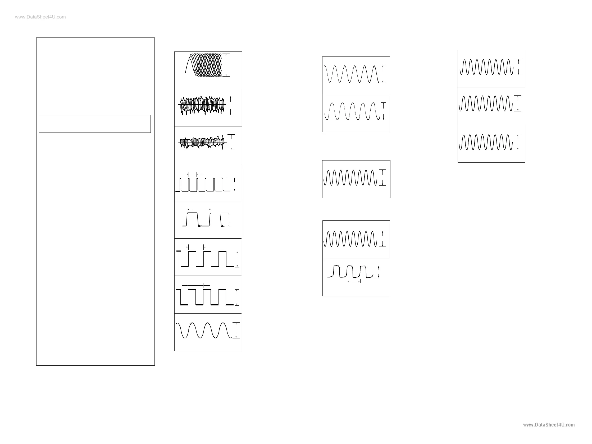
WAVEFORMS
– CD SECTION –
IC101 #£ RFO
IC101 2 FEI
IC101 $¶ TEI
IC103 ^™ RFCK
6
IC103 ^º XPCK
7
IC103 &¢ WFCK
IC103 *ª XTAI
8
500mV/DIV, 500nsec/DIV
1.3Vp-p
200mV/DIV, 1µsec/DIV
0.5Vp-p
50mV/DIV, 1msec/DIV
0.2Vp-p
7.8µsec
2.5Vp-p
230µsec
5Vp-p
135µsec
5Vp-p
135µsec
5Vp-p
16.9344MHz
2.6Vp-p
1
2
IC1752 !¢ OEC O
IC21 @¢ XOUT
– TUNER SECTION –
(AEP, UK, German model)
1
IC21 @¢ XOUT
– TUNER SECTION –
(East European, CIS model)
4.5MHz
4.2Vp-p
1
2
IC801 2 X-OUT
IC601 8 X-OUT
3
IC851 2 TX
– DISPLAY SECTION –
1
2
IC501 !£ XT2
IC501 0 X2
– MAIN SECTION –
5MHz
5.5Vp-p
32.768kHz
5Vp-p
8MHz
4Vp-p
8MHz
4.3Vp-p
4.09MHz
3.6Vp-p