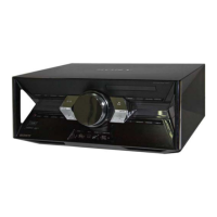
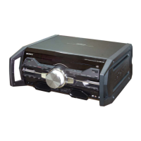
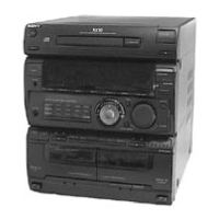
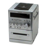
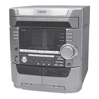
HCD-SHAKE5/SHAKE6D
59
Pin No. Pin Name I/O Description
111 ADACVSS1 - Ground terminal
112 ARF/LFE O Master clock signal output to the A/D converter and D/A converter
113 ARS O Bit clock signal output to the A/D converter and D/A converter
114 AR - Not used
115 AVCM I Audio D/A converter reference voltage terminal
116 AL - Not used
117 ALS O L/R sampling clock signal output to the A/D converter and D/A converter
118 ALF/CENTER O Audio data output to the D/A converter
119 ADACVDD1 - Power supply terminal (+3.3V)
120 ADACVDD2 - Power supply terminal (+3.3V)
121 AVDD12_1 - Power supply terminal (+1.2V)
122 AGND12 - Ground terminal
123 RFIP I AC coupled RF signal input from the optical pick-up block
124 RFIN I AC coupled RF signal input from the optical pick-up block
125 RFG I Power monitor terminal
126 RFH I Spindle motor hall sensor input from the motor driver
127 RFA I RF main beam (C) input from the optical pick-up block
128 RFB I RF main beam (B) input from the optical pick-up block