— 61 —
Pin No.
81
82
83
84
85
86
87
88
89
90
91
92
93
94
95
96
97
98
99
100
101
102
103
104
105
106
107
108
109
110
111
112
113
114
115
116
117
118
119
120
I/O
O
O
O
O
O
O
O
O
I
—
—
I
I
I
I
O
I
O
O
O
O
O
I
—
—
O
I
—
I
I
I
I
I
I
I/O
I
O
I
I
I
Description
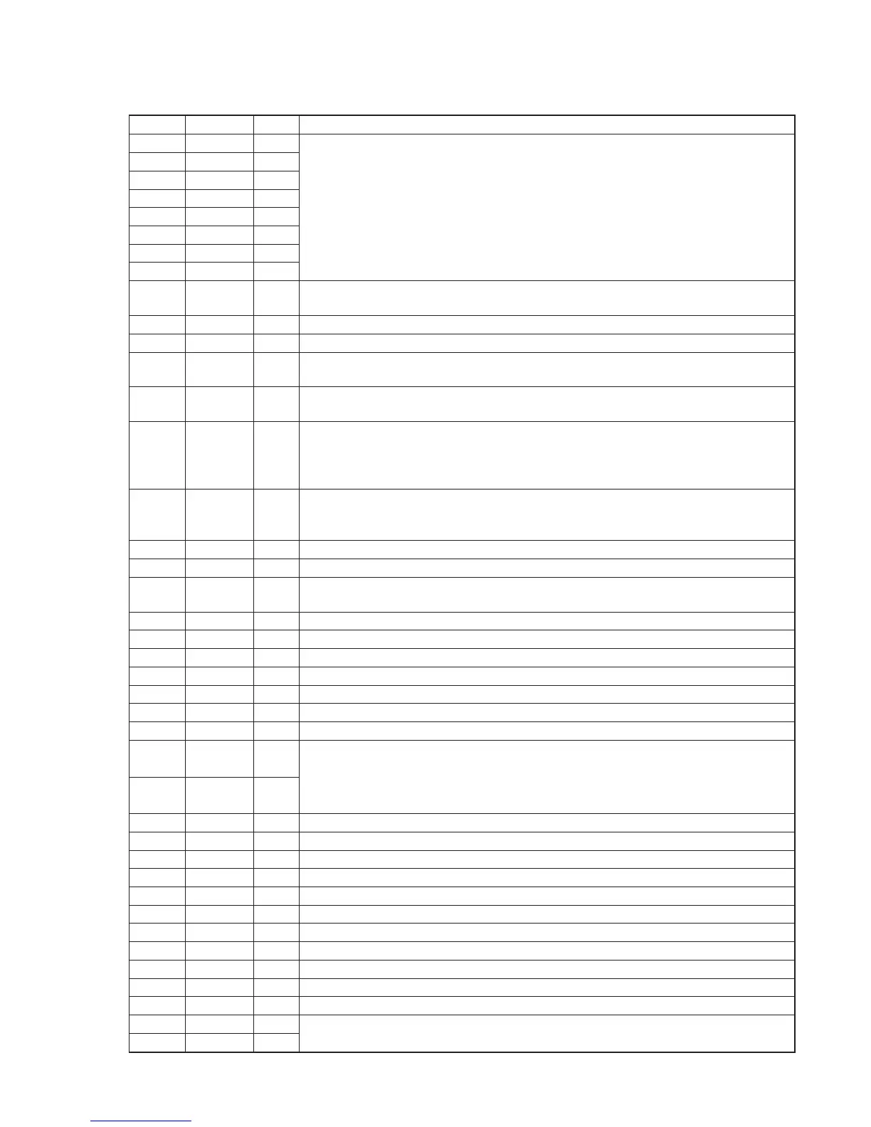
Output pin of the B or Cb signal of the image data. MSB is B/Cb7. Synchronizes with DCLK. (Not used)
Dot clock (DCLK) signal pin. The DCLK frequency is normally 13.5MHz. The DCLK can be input from this pin
or can be made by frequency-dividing (1/integer) the clock input from XTL0I.
+5V power supply
Ground
Horizontal sync signal pin. When using the built-in sync generator, a signal is made by frequency-dividing the
dot clock (DCLK). Serves as the input when not using the built-in sync generator.
Vertical sync signal pin. When using the built-in sync generator, a signal is made by frequency-dividing the
DCLK. Serves as the input when not using the built-in sync generator.
Field determination signal. Odd field correspond to “H” and even field correspond to “L”. Serves as an output
when the built-in sync generator is used, and as an input when not.
/ Signal obtained by frequency-dividing the clock input from XTL0I or XTLI. When the input clock is 8 fsc, it
can be used as the horizontal sync signal phase comparison reference signal.
Composite blanking signal pin. Serves as an output when the built-in sync generator is used, and as an input
when not. / Signal obtained by frequency-dividing the clock input from XTL0I or XTLI. When the input clock is
8 fsc, it can be used as the fsc signal.
Composite sync signal pin. A signal is made by frequency-dividing the DCLK. Cannot be input. (Not used)
Sync generator reset signal pin. The signal generator is initialized by setting this pin to “L”.
Outputs the frequency-divided clock of the clock input to XTL0I. The frequency dividing ratio can be selected
from 1/2, 1/4, and 1/8. (Not used)
Digital output (Not used)
Audio serial data output to Audio D/A converter (IC101)
LR clock output to Audio D/A converter (IC101)
Bit clock output to Audio D/A converter (IC101)
Input 384fs (16.9344MHz) or 768fs (33.8688MHz).
+5V power supply
Ground
CD-ROM decoder, audio decoder master clock. Input a clock to the XTL21 or connect an oscillator between
XTL2I and XTL2O. The recommended frequency is 45 MHz. This clock is for the internal circuit. Does not
synchronize with inputs and outputs.
+5V power supply
C2 pointer input (CXD2545Q)
LR clock input (CXD2545Q)
Serial data input (CXD2545Q)
Bit clock input (CXD2545Q)
Digital input signal (Not used)
Register access chip select signal pin.
Data acknowledge/wait signal pin for DMA transmission, register access, transparent memory access.
Register access control signal pin.
Interrupt request signal
Hardware reset input pin. When set to “L”, all registers and operations are reset and initialized.
Address input pin. In some cases, serves as the control signal and data input according to the setting
of the control mode.
Pin Name
B/Cb0
B/Cb1
B/Cb2
B/Cb3
B/Cb4
B/Cb5
B/Cb6
B/Cb7
DCLK
VDD
VSS
HSYNC
VSYNC
FID/FHREF
CBLNK/FSC
CSYNC
XSGRST
CLK0O
DOUT
DATO
LRCO
BCKO
FSXI
VDD
VSS
XTL2O
XTL2I
VDD
C2PO
LRCI
DATI
BCKI
DOIN
XHCS
XHDT
HRW
XHIRQ
XRST
HA0
HA1



 To Next Page