– 45 – – 46 – – 48 –– 47 – – 49 –
ICF-SW07
r
Waveforms (MAIN Section)
1
IC402 @¢
2
3
VOLT/DIV : 0.5 V AC
TIME/DIV : 5 µsec
Q406 C
Q408 C
VOLT/DIV : 1 V AC
TIME/DIV : 0.1 µsec
VOLT/DIV : 1 V AC
TIME/DIV : 0.2 µsec
1.8 Vp-p
75 kHz
3.8 Vp-
377 nsec
5 Vp-
594 nsec
Note:
• All capacitors are in µF unless otherwise noted. pF: µµF
50 WV or less are not indicated except for electrolytics
and tantalums.
• All resistors are in Ω and
1
/
4
W or less unless otherwise
specified.
•
¢
: internal component.
• U : B+ Line.
• H : adjustment for repair.
• Power voltage is dc 3V and fed with regulated dc power
supply from external power voltage jack.
• Voltages and waveforms are dc with respect to ground
under no-signal (detuned) conditions.
no mark : FM
( ) : MW/LW
< > : SW
[ ] :AM EXT ANT CONNECTED
• Voltages are taken with a VOM (Input impedance 10 MΩ).
Voltage variations may be noted due to normal produc-
tion tolerances.
• Waveforms are taken with a oscilloscope.
Voltage variations may be noted due to normal produc-
tion tolerances.
• Circled numbers refer to waveforms.
• Signal path.
F : FM
f : SW
L : MW/LW
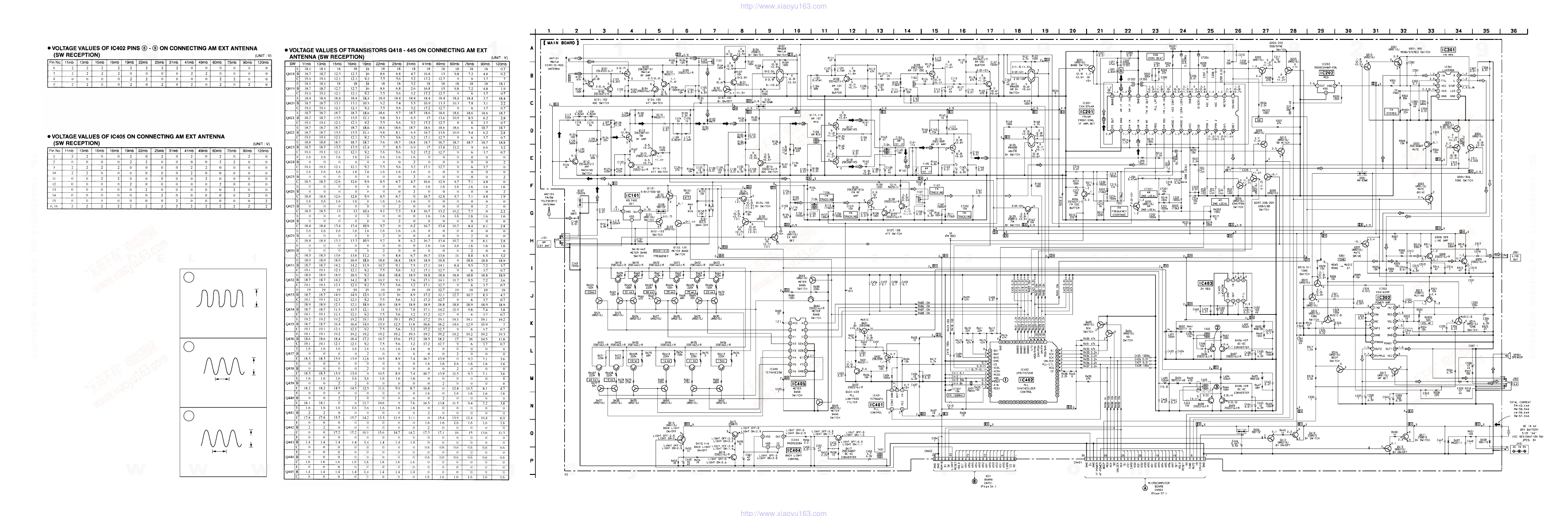
5-4. SCHEMATIC DIAGRAM (MAIN SECTION)
r
Refer to page 63 for IC Block Diagrams.
w
w
w
.
x
i
a
o
y
u
1
6
3
.
c
o
m
Q
Q
3
7
6
3
1
5
1
5
0
9
9
2
8
9
4
2
9
8
T
E
L
1
3
9
4
2
2
9
6
5
1
3
9
9
2
8
9
4
2
9
8
0
5
1
5
1
3
6
7
3
Q
Q
TEL 13942296513 QQ 376315150 892498299
TEL 13942296513 QQ 376315150 892498299
http://www.xiaoyu163.com
http://www.xiaoyu163.com