– 52 – – 53 –– 50 – – 51 – – 54 –
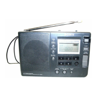
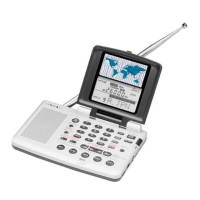
ICF-SW07
Note:
• X : parts extracted from the component side.
•
r
: Through hole.
• b : Pattern from the side which enables seeing.
(The other layers' patterns are not indicated.)
Caution:
Pattern face side: Parts on the pattern face side seen from the
(Side A) pattern face are indicated.
Parts face side: Parts on the parts face side seen from the
(Side B) parts face are indicated.
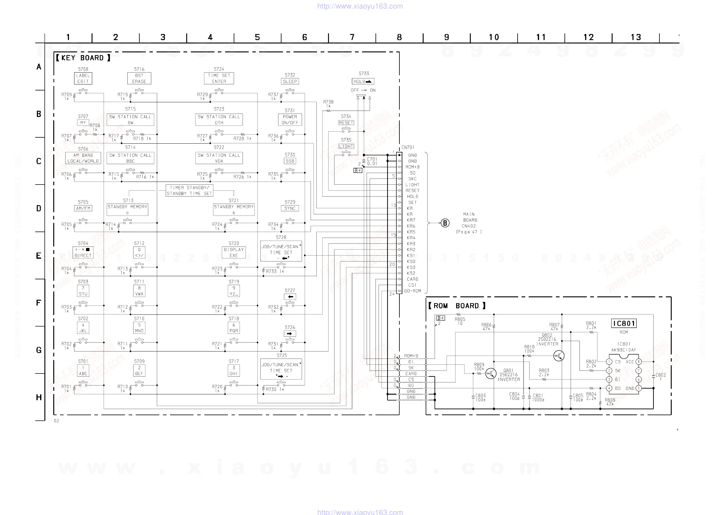
5-5. PRINTED WIRING BOARDS (KEY SECTION)
Ref. No. Location
r
Semiconductor
Location
IC801 G-12
Q801 G-12
Q802 G-12
5-6. SCHEMATIC DIAGRAM (KEY SECTION)
Note:
• All capacitors are in µF unless otherwise noted. pF: µµF
50 WV or less are not indicated except for electrolytics
and tantalums.
• All resistors are in Ω and
1
/
4
W or less unless otherwise
specified.
• U : B+ Line.
• Power voltage is dc 3V and fed with regulated dc power
supply from external power voltage jack.
• Voltages are dc with respect to ground under no-signal
(detuned) conditions.
no mark : SW
• Voltages are taken with a VOM (Input impedance 10 MΩ).
Voltage variations may be noted due to normal produc-
tion tolerances.
• The voltage isn't filled in the measurement impossibility
place.
w
w
w
.
x
i
a
o
y
u
1
6
3
.
c
o
m
Q
Q
3
7
6
3
1
5
1
5
0
9
9
2
8
9
4
2
9
8
T
E
L
1
3
9
4
2
2
9
6
5
1
3
9
9
2
8
9
4
2
9
8
0
5
1
5
1
3
6
7
3
Q
Q
TEL 13942296513 QQ 376315150 892498299
TEL 13942296513 QQ 376315150 892498299
http://www.xiaoyu163.com
http://www.xiaoyu163.com