BDP-S500
NOTE
(For printed wiring boards)
• b: Pattern from the side which enables seeing.
(The other layers’ patterns are not indicated)
• Through hole is omitted.
• Circled numbers refer to waveforms.
•There are few cases that the part printed on diagram
isn’t mounted in this model.
• Chip parts.
(For schematic diagrams)
• All capacitors are in µF unless otherwise noted. pF : µµF.
50V or less are not indicated except for electrolytics and tantalums.
• All resistors are in ohms, 1/4 W (Chip resistors : 1 /10 W) un-less
otherwise specified.
kΩ=1000Ω, MΩ=1000kΩ.
• Caution when replacing chip parts.
New parts must be attached after removal of chip.
Be careful not to heat the minus side of tantalum capacitor, be-
cause it is damaged by the heat.
• All variable and adjustable resistors have characteristic curve B,
unless otherwise noted.
• 2: nonflammable resistor
• 5: fusible resistor
• C: panel designation
• f : internal component.
• C: adjustment for repair.
• U : B+ Line
• V : B– Line
• Circled numbers refer to waveforms.
•Voltages are dc between measurement point.
• Readings are taken with a color-bar signals on Blu-ray disc.
• Readings are taken with a digital multimeter (DC 10MΩ).
•Voltage variations may be noted due to normal production toler-
ances.
THIS NOTE IS COMMON FOR WIRING BOARDS AND
SCHEMATIC DIAGRAMS
(In addition to this, the necessary note is printed in each block)
21
3
21
3
21
3
345
21
123
654
EB
C
31
5
5
2
46
123
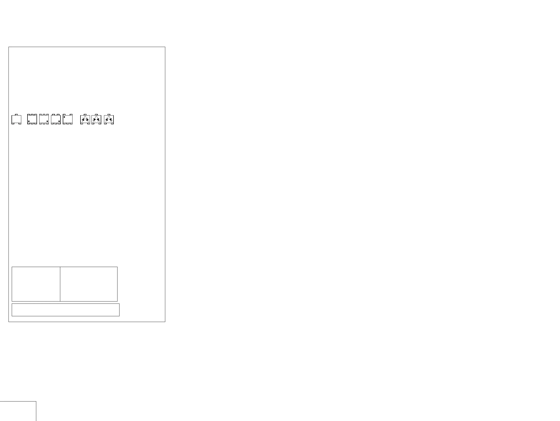
54
Transistor Diode
4-3 4-4
When indicating parts by reference number, please include
the board name.
Note:
The components identi-
fied by mark 0 or dotted
line with mark 0 are criti-
cal for safety.
Replace only with part
number specified.
Note:
Les composants identifiés par
une marque 0 sont critiques
pour la sécurité.
Ne les remplacer que par une
pièce portant le numéro
spécifié.