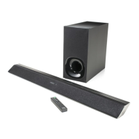
HT-CT780
HT-CT780
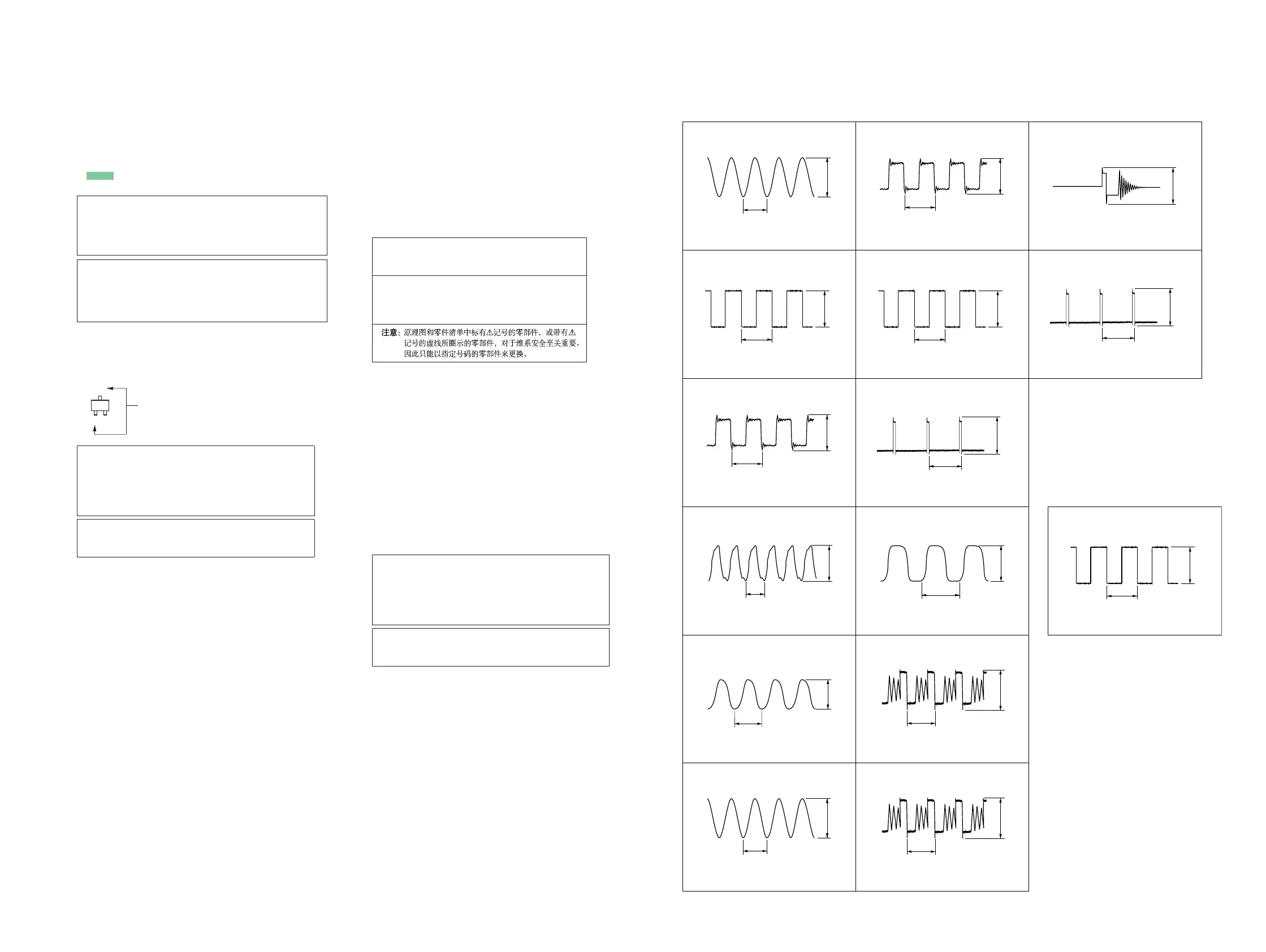
3535
7.8 Ps
12 Vp-p
wa
Q802 (BASE)
5 V/DIV, 5 Ps/DIV
20.8 Ps
3.4 Vp-p
2
IC303 qk (LRCK)
1 V/DIV, 10 Ps/DIV
3
IC303 ql (BCK)
1 V/DIV, 200 ns/DIV
324 ns
3.7 Vp-p
5
IC303 r; (XTO)
1 V/DIV, 20 ns/DIV
40.6 ns
2.6 Vp-p
qd
IC603 3 (SW1)
2 V/DIV, 1 Ps/DIV
8.2 Vp-p
qf
IC603 qf (SW2)
2 V/DIV, 1 Ps/DIV
1.6 Ps
8.3 Vp-p
qs
IC601 1 (BOOT)
5 V/DIV, 1 Ps/DIV
3 Ps
20.2 Vp-p
qa
IC602 1 (BOOT)
5 V/DIV, 1 Ps/DIV
3 Ps
20.6 Vp-p
9
IC313 1 (BOOT)
5 V/DIV, 2 Ps/DIV
2.9 Ps
21 Vp-p
6
IC308 qd (XTAL)
1 V/DIV, 20 ns/DIV
39.4 ns
3.8 Vp-p
q;
IC102 ua (X1)
1 V/DIV, 100 ns/DIV
250 ns
3.4 Vp-p
7
IC308 y; (BCLK_OUT)
1 V/DIV, 200 ns/DIV
324 ns
4.4 Vp-p
20.8 Ps
3.6 Vp-p
8
IC308 ya (LRCLK_OUT)
1 V/DIV, 10 Ps/DIV
4
IC303 w; (SCKO)
1 V/DIV, 20 ns/DIV
40.4 ns
3.1 Vp-p
1
IC1501 <zzc (XTALOUT)
1 V/DIV, 20 ns/DIV
37.4 ns
2.4 Vp-p
For Schematic Diagrams.
Note:
• All capacitors are in μF unless otherwise noted. (p: pF) 50
WV or less are not indicated except for electrolytics and
tantalums.
• All resistors are in Ω and 1/4 W or less unless otherwise
specifi ed.
•
f
: Internal component.
• 2 : Nonfl ammable resistor.
• 5 : Fusible resistor.
• C : Panel designation.
THIS NOTE IS COMMON FOR PRINTED WIRING BOARDS AND SCHEMATIC DIAGRAMS.
(In addition to this, the necessary note is printed in each block.)
• A : B+ Line.
• Voltages and waveforms are dc with respect to ground
under no-signal conditions.
no mark
: POWER ON
*
: Impossible to measure
• Voltages are taken with VOM (Input impedance 10 M).
Voltage variations may be noted due to normal production
tolerances.
• Waveforms are taken with a oscilloscope.
Voltage variations may be noted due to normal production
tolerances.
• Circled numbers refer to waveforms.
• Signal path.
F : AUDIO (ANALOG)
J : AUDIO (DIGITAL)
E : VIDEO
N : Bluetooth
For Printed Wiring Boards.
Note:
• X : Parts extracted from the component side.
• Y : Parts extracted from the conductor side.
•
f
: Internal component.
• : Pattern from the side which enables seeing.
(The other layers’ patterns are not indicated.)
Caution:
Pattern face side:
(SIDE B)
Parts face side:
(SIDE A)
Parts on the pattern face side seen
from the pattern face are indicated.
Parts on the parts face side seen from
the parts face are indicated.
• Indication of transistor.
C
B
These are omitted.
E
Q
Caution:
Pattern face side:
(Conductor Side)
Parts face side:
(Component Side)
Parts on the pattern face side seen
from the pattern face are indicated.
Parts on the parts face side seen from
the parts face are indicated.
• MAIN board is multi-layer printed board. However, the
patterns of intermediate layers have not been included in
diagrams.
• Waveforms
– MAIN Board –
– FL Board –
Note 1: When the complete MAIN board is replaced, refer
to “NOTE OF REPLACING THE IC503 ON THE
MAIN BOARD AND THE COMPLETE MAIN
BOARD” and “NOTES ON THE WIRELESS CON-
NECTION (LINK) AFTER REPAIRS ARE COM-
PLETE” on page 5.
Note 2: When the complete POWER board is replaced, refer
to “BOND FIXATION OF ELECTRIC PARTS” on
page 6.
Note: The components identifi ed by mark 0 or
dotted line with mark 0 are critical for safety.
Replace only with part number specifi ed.
Note: Les composants identifi és par une marque
0 sont critiques pour la sécurité.
Ne les remplacer que par une piéce portant
le numéro spécifi é.
Ver. 1.1