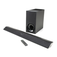
HT-CT780
55
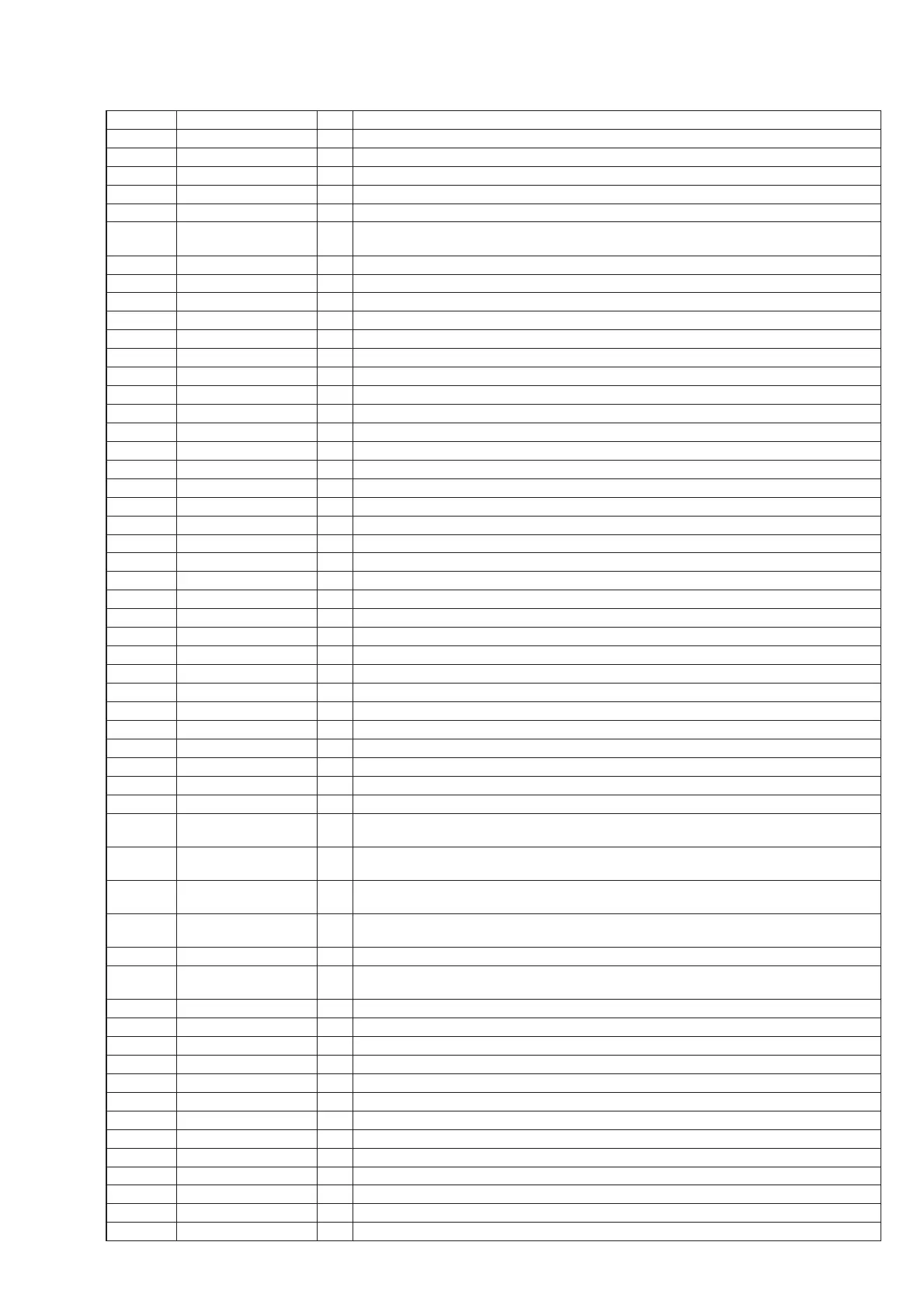
Pin No. Pin Name I/O Description
55 DAMP_SDAO I/O Two-way data bus with the stream processor
56 DRIVE_OCP (DIAG) I Shut down signal input from the digital power amplifi er “L”: shut down
57 AMP_OVF1 I Overfl ow detection signal input from the digital power amplifi er
58 HDMI_IN1_INT I Interrupt signal input from the HDMI receiver
59 HDMI_IN1_RESET O Reset signal output to the HDMI receiver “H”: reset
60 5VPWR O
+5V power on/off control signal output terminal for the ARC HDCP 2.2 HDMI OUT connector
“H”: power on
61 SPARTA_PCONT O Power on/off control signal output terminal for the HDMI section “H”: power on
62 HDMI_NLPCM O Audio setting signal output terminal “L”: LPCM audio, “H”: HBR audio
63 to 67 NO USE O Not used
68 MD1 I Mode selection signal input terminal “L”: fl ash memory writing mode
69 MD0 I Mode selection signal input terminal “H”: fl ash memory writing mode
70 X0 I System clock input terminal (4 MHz)
71 X1 O System clock output terminal (4 MHz)
72 VSS - Ground terminal
73 VCC - Power supply terminal (+3.3V)
74 PCONT_IR O Not used
75 NO USE O Not used
76 P_CONT_DSP O Power on/off control signal output terminal for the DSP “H”: power on
77 NO USE O Not used
78 Update UART Rx I Update data input terminal Not used
79 Update UART Tx O Update data output terminal Not used
80 NO USE O Not used
81 MODEL I Model setting terminal
82 DESTINATION I Destination setting terminal
83 TEMP_SENSOR I Temperature sensor input terminal Not used
84 NO USE O Not used
85 SIRCS_IN_1 I SIRCS signal input from the remote control receiver
86 NO USE O Not used
87 SIRCS_IN_2 I SIRCS signal input terminal Not used
88 KEY2 I Top panel key input terminal
89 KEY0 I Power key input terminal
90 AVCC - Power supply terminal (+3.3V)
91 AVSS - Ground terminal
92 AVRL I Reference voltage (0V) input terminal
93 AVRH I Reference voltage (+3.3V) input terminal
94 KEY1 I Top panel key input terminal
95
ACCELEROMETER_
SDA
I/O Two-way data bus terminal Not used
96
ACCELEROMETER_
SCL
O Serial data transfer clock signal output terminal Not used
97
HDMI (9575+9679)_
SCL
O Serial data transfer clock signal output to the HDMI receiver and HDMI transceiver
98
HDMI(9575+9679)_
SDA
I/O Two-way data bus with the HDMI receiver and HDMI transceiver
99 HDMI (9575) INT I Interrupt signal input from the HDMI receiver
100
ON CHIP DEBUG/
CLK1
I Serial data transfer clock signal input terminal for fl ash memory writing
101 (PROG_VUTX) O Serial data output terminal for fl ash memory writing
102 (PROG_VURX) I Serial data input terminal for fl ash memory writing
103 AC_CUT I AC cut detection signal input terminal “L”: AC cut is detected
104 HDMI (9575) RESET O Reset signal output to the HDMI transceiver “H”: reset
105 HDMI_MUTE_DET I HDMI muting on/off control signal input from the HDMI transceiver “H”: muting on
106 HDMI_MUTE_ON O HDMI muting on/off control signal output terminal “H”: muting on
107 VCC - Power supply terminal (+3.3V)
108 VSS - Ground terminal
109 VCC - Power supply terminal (+3.3V)
110 TRSTX I Test reset signal input terminal (for JTAG) Not used
111 TCK I Test clock signal input terminal (for JTAG) Not used
112 TDI I Test data input terminal (for JTAG) Not used
113 TMS I Test mode selection signal input terminal (for JTAG) Not used