– 15 – – 16 –
THIS NOTE IS COMMON FOR PRINTED WIRING
BOARDS AND SCHEMATIC DIAGRAMS.
(In addition to this, the necessary note is printed
in each block.)
For schematic diagrams.
Note:
• All capacitors are in µF unless otherwise noted. pF: µµF
50 WV or less are not indicated except for electrolytics
and tantalums.
• All resistors are in Ω and
1
/4
W or less unless otherwise
specified.
•
¢
: internal component.
• 2 : nonflammable resistor.
• C : panel designation.
• U : B+ Line.
• V : B– Line.
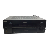
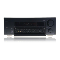
• Voltages and waveforms are dc with respect to ground
under no-signal (detuned) conditions.
no mark : FM
• Voltages are taken with a VOM (Input impedance 10 MΩ).
Voltage variations may be noted due to normal produc-
tion tolerances.
• Waveforms are taken with a oscilloscope.
Voltage variations may be noted due to normal produc-
tion tolerances.
• Circled numbers refer to waveforms.
• Signal path.
F : FM
L : AUDIO
g : VIDEO
i : SURROUND
d : PB (TAPE)
G : REC (TAPE)
p : Y
l : CHROMA
J : CD
I : PHONO
E : PB (MD/DAT)
a : REC (MD/DAT)
c : DIGITAL OUT
N : DIGITAL IN
For printed wiring boards.
Note:
• X : parts extracted from the component side.
• Y : parts extracted from the conductor side.
•
p : parts mounted on the conductor side.
•
¢
: internal component.
• b : Pattern from the side which enables seeing.
• Indication of transistor
Note: The components identified by mark ! or dotted line
with mark ! are critical for safety.
Replace only with part number specified.
1
2
IC103 !¡ X2
IC102 *™ XO
WAVEFORMS
– DISPLAY SECTION –
1
IC1 !£
– TUNER SECTION –
1
2
IC1101 @¶ X OUT
IC1201 (™ XO
– DIGITAL SECTION –
3
4
IC1101 #¢ BCK
IC1101 @ª CLK OUT
5
6
IC1403 0 2QB
IC1101 #§ LRCK
7
8
IC1305 6
IC1305 !¡, !™