4-4
UP-895/(E)
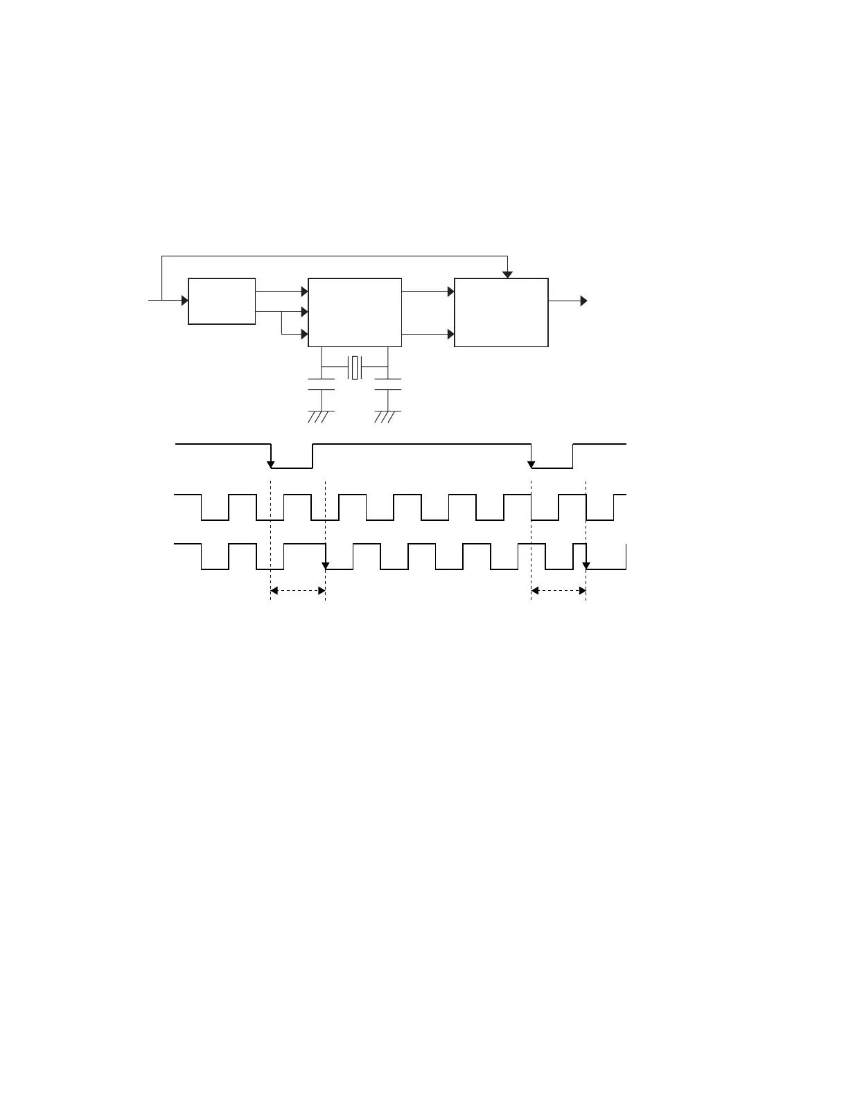
4-2. Clock Generator Circuit
A clock is generated by attaching a 23 MHz external oscillator (X500) to the clock generator circuit
(IC505). This clock is phase-adjusted at the falling edge of an H sync pulse (nINTOUT2) when fetching
a video signal. The noise contained in the clock signal generated at that time is eliminated by the internal
circuit of a memory and head control circuit (IC501) and a delay circuit (IC504). By using the clock
signal as a main clock, memory control is performed during image fetching.
Clock Generator Circuit
4-3. Memory and Head Control Circuit
The memory and head control circuit (IC501) consists of the following blocks.
The operation in each block is determined by the serial data from a system control (IC304).
(1) Register for storing the serial data from system control (IC304)
(2) Frame memory write and read control
(3) Thermal head control
(4) Sync signal processing circuit
(5) Line memory (for calculation and print)
(6) Sharpness calculation circuit
(7) Thermal storage correction calculation circuit
(8) Count correction calculation circuit
(9) Image scaling calculation circuit
nINTOUT2
CLKOUT
(Normal)
CLKOUT
(During image
fetching)
Phase adjustment Phase adjustment
nINTOUT2
DELAY
LINE
CLK
GENERATOR
IC
MEMORY
& HEAD
CONTROL
IC
CLKOUT
23M