WM-FX373/FX375
– 15 –
– 16 –
– 17 –
– 18 –
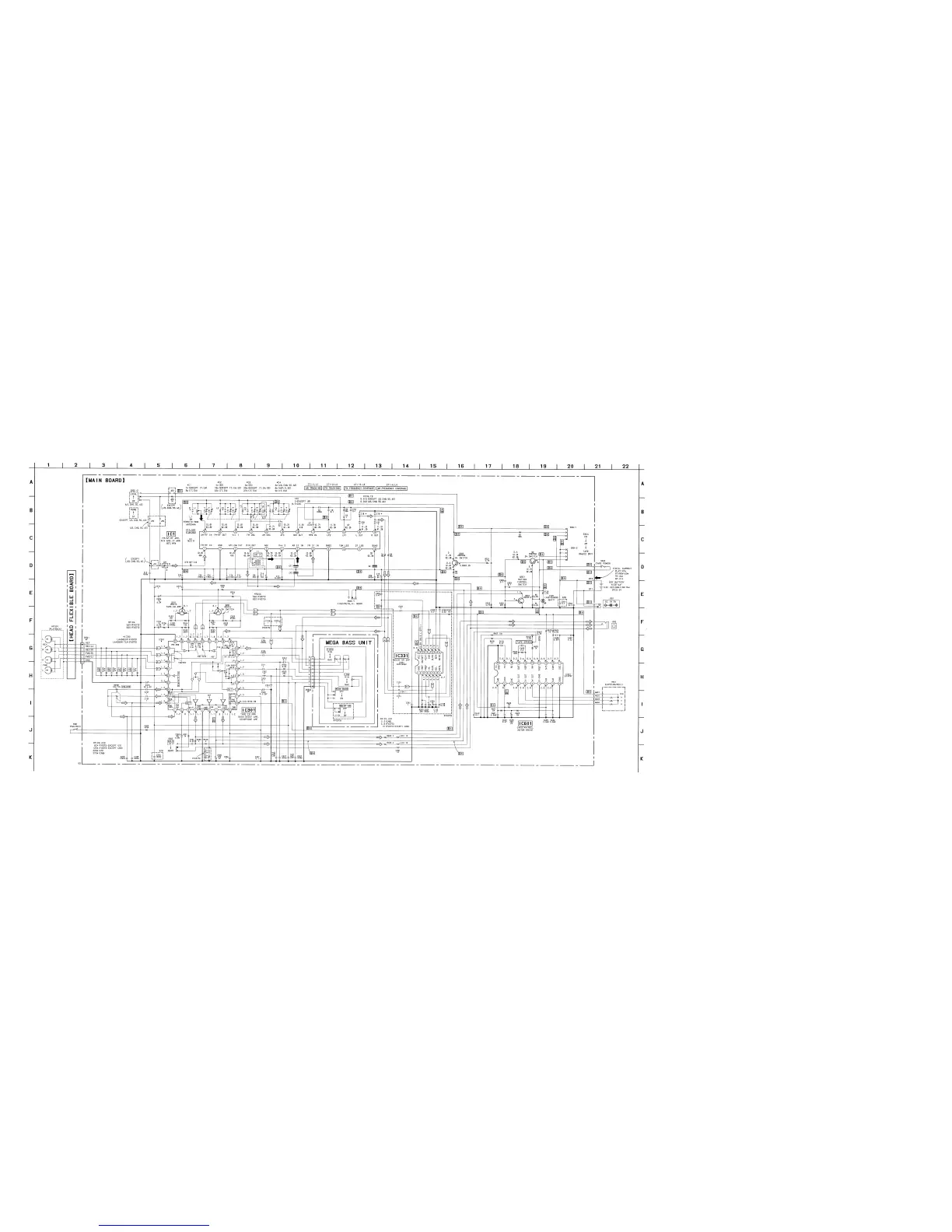
5-3. SCHEMATIC DIAGRAM • See page 19 for IC Block Diagrams.
Note on Schematic Diagram:
• All capacitors are in µF unless otherwise noted. pF: µµF
50 WV or less are not indicated except for electrolytics
and tantalums.
• All resistors are in Ω and
1
/
4
W or less unless otherwise
specified.
• f : internal component.
• C : panel designation.
• U : B+ Line.
• H : adjustment for repair.
• Power voltage is dc 3 V and fed with regulated dc power
supply from external power voltage jack.
• Voltages are dc with respect to ground under no-signal
(detuned) conditions.
no mark : PB (TAPE)
( ) : FM
〈〈 〉〉 : AM
• Voltages are taken with a VOM (Input impedance 10 MΩ).
Voltage variations may be noted due to normal produc-
tion tolerances.
• Signal path.
F : FM
f : AM
E : PB (TAPE)
• Abbreviation
CND : Canadian model.
EA : Saudi Arabia model.
EE : East European model.
IT : Italian model.
E : Radio Section (ST/MONO)
5E, 6E : Radio Section (DX/LOCAL)
Ver 1.2

 Loading...