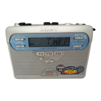
10
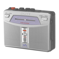
WM-GX410
SECTION 4
DIAGRAMS
Pin No. Pin name I/O Description
1 XOUT O Connected to 75kHz Crystal oscillator
2 TEST 2 I For Test (Connected to GND)
3 MECHA REC I REC mode signal input
4 to 6 PA3 to 1 I Control key inputs
7 KO2 O Key source signal output
8 KO1 O Key source signal output
9 REC CTRL O REC control signal output L: REC
10 AMP ON O Power amplifier on/off control signal output
11 SD I SD input
12 COMP I COMP input
13 PUSH I Tuning dial (S701) common switch signal input
14 MECHA TAPE I Tape on/off detection signal input
15 RADIO ON O Radio on/off control signal output
16 BAND O Band select signal output
17 TUNING-B I Tuning dial (S701) B phase signal input
18 TUNING-A I Tuning dial (S701) A phase signal input
19 MUTE O Mute signal output
20 BEEP O Beep signal output
21 BACK UP VOLTAGE I Back-up voltage detection signal input
22 BATT LEVEL I Battery voltage detection signal input
23 VERSION I Destination select signal input
24 GND — Ground terminal
25 TUNER MODE INPUT I Tuning mode select switch (S707) signal input
26 2X INPUT I Tape speed select switch (S706) signal input
27 PAUSE I Pause switch (S702) signal input
28 HOLD I HOLD switch (S705) signal input
29 SHUTDOWN O Not used (open)
30 MOTOR BRAKE O Motor brake control signal output
31 MOTOR CTL O Motor control signal output
32 to 44 S13 to S1 O LCD driver segment output terminal
45 to 48 COM4 to 1 O LCD driver common output terminal
49 TU O Output for tuning voltage generator
50 to 53 DBR4 to 1 I For LCD power supply booster
54 RESET I System reset signal input
55 HCTR NC — Not used (open)
56 VDD — Power supply terminal
57 FM IN I FM VCO input
58 AM IN I AM VCO input
59 GND — Ground terminal
60 E0 O Tuning signal (PWM) output
61 AIN I LPF amplifier input
62 AOUT O LPF amplifier output
63 TEST 1 I For test (connected to ground)
64 XIN I Connected to 75kHz Crystal oscillator
4-1. IC Pin Function Descriptions
IC701 (SYSTEM CONTROL/LCD DRIVE) LC723483 W-9C33-E
 Loading...