21
WM-GX410
Common Note on Schematic Diagram:
• All capacitors are in µF unless otherwise noted. pF: µµF
50 WV or less are not indicated except for electrolytics
and tantalums.
• All resistors are in W and
1
/
4
W or less unless otherwise
specified.
• C : panel designation.
• A : B+ Line.
• H : adjustment for repair.
• Power voltage is dc 3V and fed with regulated dc power
supply from battery terminal.
•Voltage and waveforms are dc with respect to ground
under no-signal (detuned) conditions.
no mark : FM
() : AM
< > : REC
[] : PB
•Voltages are taken with a VOM (Input impedance 10 MΩ).
Voltage variations may be noted due to normal produc-
tion tolerances.
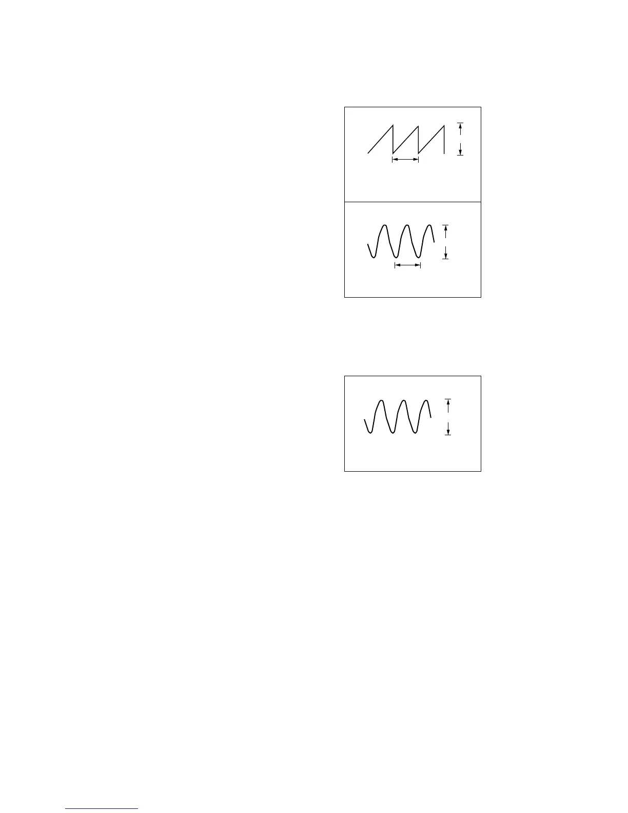
•Waveforms are taken with a oscilloscope.
Voltage variations may be noted due to normal produc-
tion tolerances.
• Circled numbers refer to waveforms.
• Signal path.
F : FM
f : AM
E : PB
a : REC
N : MIC
• Abbreviation
CND : Canadian
EA : Saudi Arabia
CH : Chinese
JEW : Tourist
5E : Indication of country of origin
9E : No Indication of country of origin
– MAIN SECTION –
 Loading...