UM1670 Rev 4 21/32
UM1670 Hardware layout
31
6.13 Solder bridges
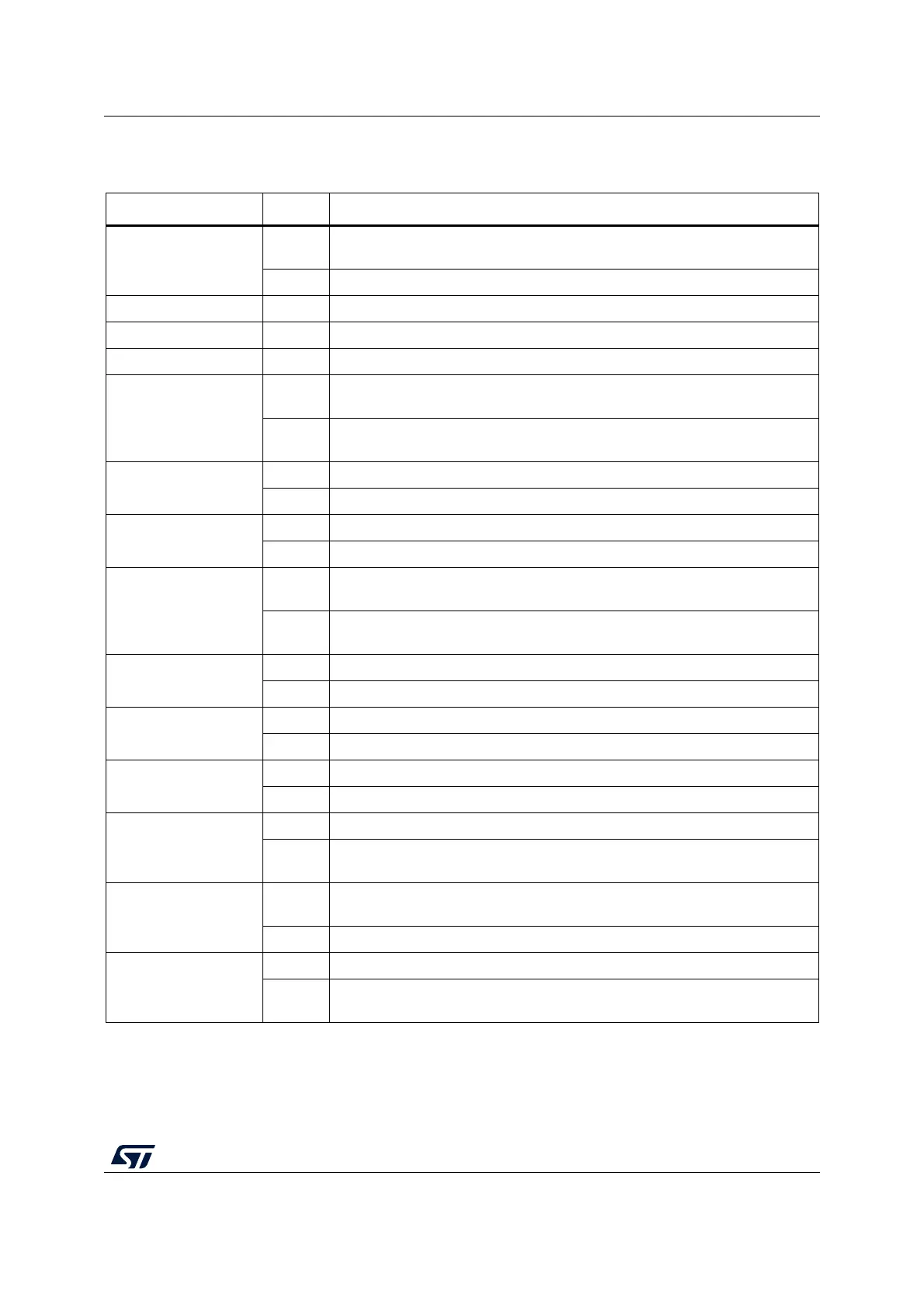
Table 6. Solder bridges
Bridge State
(1)
1. The default SBx state is shown in bold.
Description
SB19, 20 (X3 crystal)
OFF
X3, C20, C21, R56, and R57 provide a clock. PH0 and PH1 are disconnected
from P2.
ON PH0 and PH1 are connected to P2. Remove only R56 and R57.
SB4, 6, 8,14 (default) ON Reserved, do not modify.
SB3, 5, 7,13 (reserved) OFF Reserved, do not modify.
SB22, 23, 24, 25 OFF Reserved, do not modify.
SB16, 17 (X2 crystal)
OFF
X2, C23, C24, R53, and R54 deliver a 32 kHz clock.
PC14 and PC15 are not connected to P2
ON
PC14 and PC15 are only connected to P2.
Remove only R53 and R54.
SB1 (B2-RESET)
ON B2 push-button is connected to the NRST of STM32F429ZIT6.
OFF B2 push-button is not connected to the NRST of STM32F429ZIT6.
SB2 (B1-USER)
ON B1 push-button is connected to PA0.
OFF B1 push-button is not connected to PA0.
SB11, 15 (RX,TX)
OFF
STM32F429 USART1 is not connected to ST-LINK, so VCP is disabled
(Default configuration on 32F429IDISCOVERY).
ON
STM32F429 USART1 is connected to ST-LINK, so VCP is enabled (default
configuration on STM32F429I-DISC1).
SB12 (NRST)
ON NRST signal of connector CN2 is connected to the NRST of STM32F429ZIT6.
OFF NRST signal is not connected.
SB9 (SWO)
OFF SWO signal is not connected.
ON SWO signal of connector CN2 is connected to PB3.
SB10 (STM_RST)
OFF No incidence on the NRST signal of STM32F429ZIT6.
ON NRST signal of STM32F429ZIT6 is connected to GND.
SB21 (BOOT0)
ON BOOT0 signal of STM32F429ZIT6 is at level LOW through 510
Ω pull-down.
OFF
BOOT0 signal of STM32F429ZIT6 is at level HIGH through 10 K
Ω pull-up (not
provided).
SB26, 27 (USB OTG)
OFF
PB14 and PB15 are only used for USB OTG and not connected to P2 to avoid
noise.
ON PB14 and PB15 are connected to P2.
SB18 (MCO)
OFF MCO signal of STM32F429ZIT6 is not used.
ON
MCO clock signal from STM32F429ZIT6 is connected to OSC_IN of
STM32F429ZIT6.