Hardware layout and configuration UM1956
24/37 UM1956 Rev 5
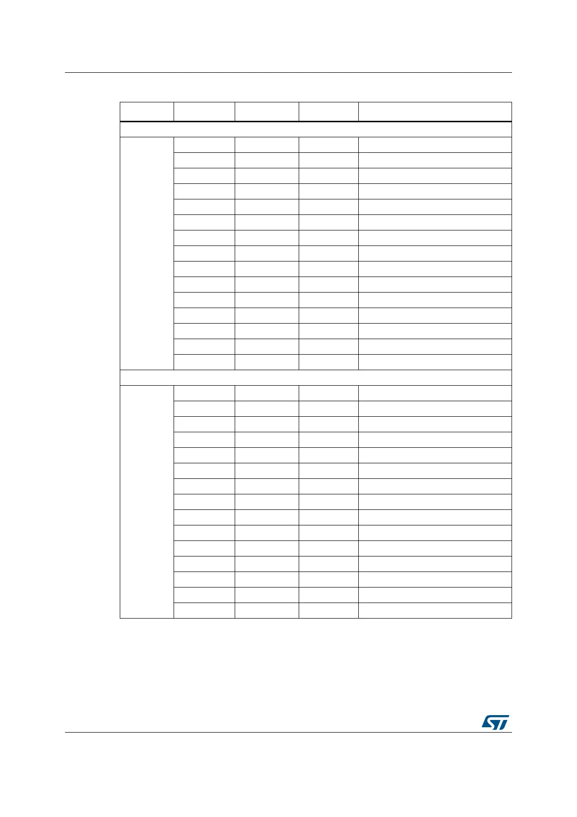
Table 11. Arduino Nano connectors on NUCLEO-F301K8
Connector Pin number Pin name STM32 pin Function
Left connector
CN3
1 D1 PA9 USART1_TX
2 D0 PA10 USART1_RX
3 RESET NRST RESET
4 GND - Ground
5 D2 PA12 -
6 D3 PB0 TIM1_CH2N
(1)
1. D3, D5, and D6 PWM on inverted channel.
7 D4
(2)
2. Limitations on A4 and A5, D4 and D5, related to I
2
C configuration, are explained in Section 6.10: Solder
bridges according to SB16/SB18 setting.
PB7 -
8 D5
(2)
PB6 TIM16_CH1N
(1)
9 D6 PB1 TIM1_CH3N
(1)
10 D7
(3)
3. D7/D8 shared with OSC_IN/OSC_OUT.
PF0 -
11 D8
(3)
PF1 -
12 D9 PA8 TIM1_CH1
13 D10 PA11 SPI_CS
(4)
4. SPI_CS is made by GPIO.
|| TIM1_CH4
14 D11 PB5 SPI3_MOSI || TIM17_CH1
15 D12 PB4 SPI3_MISO
Right connector
CN4
1 VIN - Power input
2 GND - Ground
3 RESET NRST RESET
4 +5V - 5 V input/output
5 A7 PA2 ADC1_IN3
(5)
5. PA2 exclusive with VCP_TX.
6 A6 PA7 ADC1_IN5
7 A5
(2)
PA6 ADC1_IN10 || I2C1_SCL
8 A4
(2)
PA5 ADC
(6)
|| I2C1_SDA
6. No ADC on A4.
9 A3 PA4 ADC1_IN5
10 A2 PA3 ADC1_IN4
11 A1 PA1 ADC1_IN2
12 A0 PA0 ADC1_IN1
13 AREF - AVDD
14 +3V3 - 3.3 V input/output
15 D13 PB3 SPI3_SCK

 Loading...


