Debug management
20/29 AN2586 Rev 8
5.3.3 Internal pull-up and pull-down resistors on JTAG pins
The JTAG input pins must not be floating since they are directly connected to flip-flops to
control the debug mode features. Special care must be taken with the SWCLK/TCK pin that
is directly connected to the clock of some of these flip-flops.
To avoid any uncontrolled I/O levels, the STM32F10xxx embeds internal pull-up and pull-
down resistors on JTAG input pins:
• JNTRST: Internal pull-up
• JTDI: Internal pull-up
• JTMS/SWDIO: Internal pull-up
• TCK/SWCLK: Internal pull-down
Once a JTAG I/O is released by the user software, the GPIO controller takes control again.
The reset states of the GPIO control registers put the I/Os in the equivalent state:
• JNTRST: Input pull-up
• JTDI: Input pull-up
• JTMS/SWDIO: Input pull-up
• JTCK/SWCLK: Input pull-down
• JTDO: Input floating
The software can then use these I/Os as standard GPIOs.
Note: The JTAG IEEE standard recommends to add pull-up resistors on TDI, TMS and nTRST,
but there is no special recommendation for TCK. However, for the STM32F10xxx, an
integrated pull-down resistor is used for JTCK. Having embedded pull-up and pull-down
resistors removes the need for external resistors.
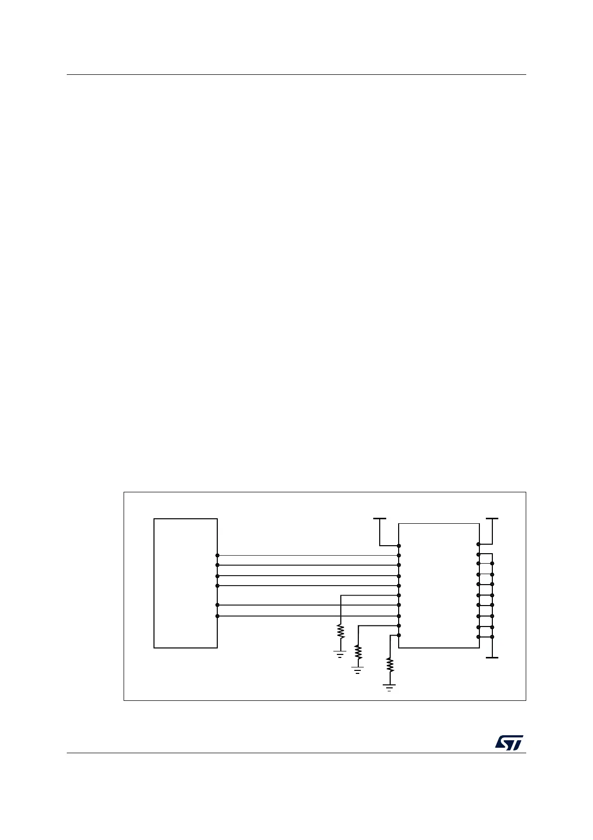
5.3.4 SWJ debug port connection with standard JTAG connector
Figure 12 shows the connection between the STM32F10xxx and a standard JTAG
connector.
Figure 12. JTAG connector implementation
ai14376
V
DD
V
DD
STM32F10xxx
nJTRST
JTDI
JSTM/SWDIO
JTCK/SWCLK
JTDO
nRSTIN
(1) VTREF
(3) nTRST
(5) TDI
(7) TMS
(9) TCK
(11) RTCK
(13)TDO
(15) nSRST
(17) DBGRQ
(19) DBGACK
10 kΩ
10 kΩ
10 kΩ
V
SS
(2)
(4)
(6)
(8)
(10)
(12)
(14)
(16)
(18)
(20)
Connector 2 × 10
JTAG connector CN9
 Loading...


