AN2586 Rev 8 9/29
Power supplies
28
Figure 2. Power supply scheme
1. Optional. If a separate, external reference voltage is connected on V
REF+
, the two capacitors (100 nF and
1 µF) must be connected.
2. V
REF
+ is either connected to V
DDA
or to V
REF
.
3. N is the number of V
DD
and V
SS
inputs.
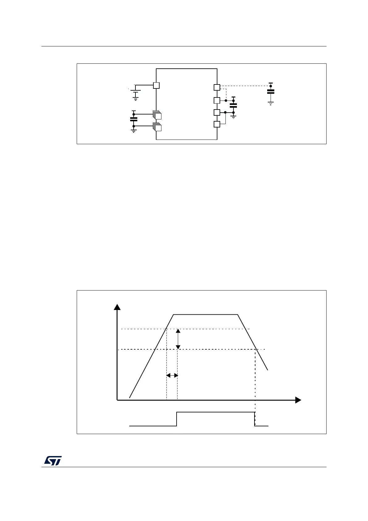
2.3 Reset and power supply supervisor
2.3.1 Power on reset (POR) / power down reset (PDR)
The device has an integrated POR/PDR circuitry that allows proper operation starting from
2V.
The device remains in the Reset mode as long as V
DD
is below a specified threshold,
V
POR/PDR
, without the need for an external reset circuit. For more details concerning the
power on/power down reset threshold, refer to the electrical characteristics in the low-
density, medium-density, high-density, XL-density, and connectivity line STM32F10xxx
datasheets.
Figure 3. Power on reset/power down reset waveform
V
BAT
STM32F10xxx
N × 100 nF
V
DD
+ 1 × 10 µF
100 nF + 1 µF
100 nF + 1 µF
(note 1)
Battery
V
BAT
V
REF+
V
DDA
V
SSA
V
REF–
V
DD 1/2/3/.../N
V
SS 1/2/3/.../N
V
REF
V
DD
ai14865b
VDD/VDDA
40 mV
hysteresis
PDR
PDR
MS30431V2
Reset
Temporization
tRSTTEMPO
VPOR/PDR
rising edge
VPOR/PDR
falling edge
 Loading...


