AN2586 Rev 8 7/29
Power supplies
28
2 Power supplies
2.1 Introduction
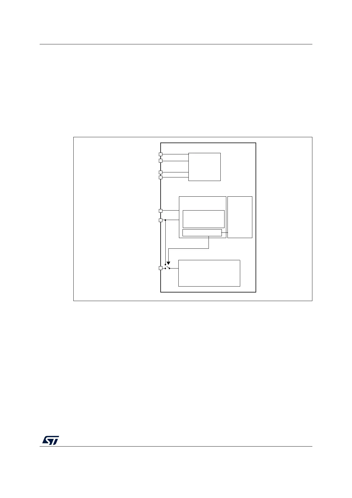
The device requires a 2.0 to 3.6 V operating voltage supply (V
DD
). An embedded regulator
is used to supply the internal 1.8 V digital power.
The real-time clock (RTC) and backup registers can be powered from the V
BAT
voltage
when the main V
DD
supply is powered off.
Figure 1. Power supply overview
Note: V
DDA
and V
SSA
must be connected, respectively, to V
DD
and V
SS
.
2.1.1 Independent A/D converter supply and reference voltage
To improve the conversion accuracy, the ADC has an independent power supply that can be
filtered separately, and shielded from noise on the PCB:
• the ADC voltage supply input is available on a separate V
DDA
pin
• an isolated supply ground connection is provided on the V
SSA
pin
When available (depending on package), V
REF–
must be tied to V
SSA
.
On 100- and 144-pin packages
To ensure a better accuracy on low-voltage inputs, the user can connect a separate external
reference voltage ADC input on V
REF+
. The voltage on V
REF+
can range from 2.4 V to V
DDA
.
A/D converter
V
DD
V
SS
I/O Ring
BKP registers
Temp. sensor
Reset block
Standby circuitry
PLL
(Wakeup logic,
IWDG)
RTC
Voltage regulator
Core
memories'
digital
peripherals
Low voltage detector
(V
SSA
) V
REF–
V
DDA
domain
V
DD
domain
1.8 V domain
Backup domain
LSE crystal 32 KHz oscillator
RCC BDCR register
ai14863
(from 2.4 V up to V
DDA
) V
REF+
(V
DD
) V
DDA
(V
SS
) V
SSA
(V
DD
) V
BAT
 Loading...


