EasyManua.ls Logo

ST STM32L152-EVAL User Manual

ST STM32L152-EVAL
44 pages
To Next Page IconTo Next Page
To Previous Page IconTo Previous Page
Page #17 background image
UM1018 Hardware and layout
Doc ID 18141 Rev 1 17/44
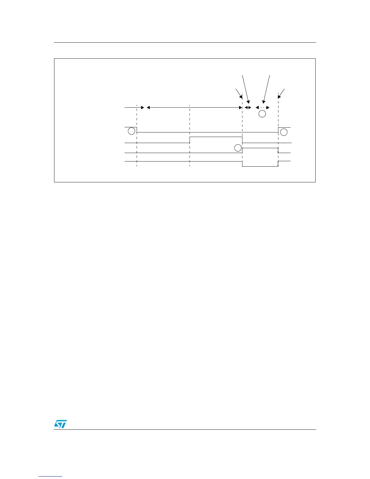
Figure 5. STM32L152-EVAL IDD low power modes measurement timing diagram
The principle used to measure a current when the STM32L is in Low power mode is:
1. Configure ADC to measure voltage on the IDD_Measurement pin (PA5).
2. Configure PA0 to serve as wakeup pin.
3. Enter Low power mode after setting IDD_CNT_EN signal low.
4. IDD_WAKEUP rising edge wakes up the MCU after around 300 ms.
5. Start ADC conversion as soon as possible after wakeup in order to measure the
voltage corresponding to Low power mode on capacitor C25.
6. Reset the counter by programming IDD_CNT_EN high (in less than 70 ms after the
wakeup) to avoid the R35 (1 KOhm) resistor being connected later in Run mode.
In Low power modes, the 1 KOhm resistor is connected when T4 goes off after entering Low
power mode. Q12 output of the counter allows connection of the 1 K resistor when the
current IDD becomes very low.
Figure 5 shows how the counter and T4 ensure that, 150 ms after IDD_CNT_EN falling
edge, the shunt resistor R35 is connected between VDD_MCU and the power supply in
order to reduce the measurement range to 30 uA full scale when VDD = 1.8 V.
Then after another 150 ms for current stabilization, R35 is shorted, the IDD measurement is
stored in C25, and the MCU is woken up.
After wakeup the MCU can measure the IDD current corresponding to the Low power mode
stored in C25.
Note: It is recommended to maintain VDD on the STM32L at a value lower than 3.5 V during low
power current measurement to avoid extra current consumption on the NRST pin (U11 pin
14).
The reason for this is that the NRST pin of the STM32L is connected to the ST-LINK MCU
T_NRST signal (U23 pin 18), and as the ST-LINK is powered at 3.3 V a leakage current is
injected into the STM32L NRST pin when MCU VDD becomes equal to or greater than
3.5 V.
MCU mode Run Stop or Standby
Wake-up Clear CNT
IDD_CNT_EN (PB15)
Q12 = LOW_POWER_EN
(T4 pin 3)
Q13 = IDD_WAKEUP
Q13n = disconnect filter
0ms
150 ms
300 ms
event event
Wake-up
period
IDD
measurement
3
4
5
6
(U7 pin 4)
(PC13)
Downloaded from Elcodis.com electronic components distributor

Other manuals for ST STM32L152-EVAL

Question and Answer IconNeed help?

Do you have a question about the ST STM32L152-EVAL and is the answer not in the manual?

ST STM32L152-EVAL Specifications

General IconGeneral
CoreARM Cortex-M3
Operating FrequencyUp to 32 MHz
Flash Memory128 KB
I/O PortsYes
GPIO PinsUp to 51
ADC12-bit
ADC ChannelsUp to 16
DAC Channels2
Communication InterfacesI2C, SPI, USART
USBUSB 2.0 full-speed
ConnectorsUSB
On-board FeaturesLEDs, buttons, joystick
LCD DriverYes
Operating Temperature-40°C to +85°C

Summary

Hardware and Layout

Development and Debug Support

Embedded ST-LINK/V2 for on-board program loading and debugging via JTAG or SWD.

Power Supply

Details on powering the board via various sources and associated LEDs.

Clock Source

Information on the two available clock sources: 32 KHz crystal and 8 MHz crystal.

Reset Source

Lists the various sources that can trigger a reset on the evaluation board.

IDD Measurement

Built-in circuit for measuring MCU current consumption in Run or Low power modes.

Connectors

ST-LINK/V2 USB Type B Connector CN11

USB connector for connecting the embedded ST-LINK/V2 to a PC for debugging.

User USB Type B Connector CN1

USB connector for user interaction and potentially powering the board.

JTAG Connector CN9

Connector for JTAG debugging interface.

Trace Debugging Connector CN8

Connector for trace debugging functionality.

Related product manuals