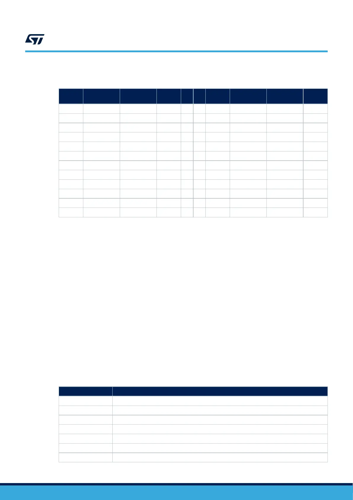
Table 10 describes the pinout of USB Type-C
®
connector CN7.
Table 10. CN7 USB Type-C
®
connector pinout
Function STM32 pin Signal name
Pin
name
Pin Pin
Pin
name
Signal name STM32 pin Function
GND - GND GND A1 B12 GND GND - GND
TX1+ - - TX1+ A2 B11 RX1+ - - RX1+
TX1- - - TX1- A3 B10 RX1- - - RX1-
VBUS - - VBUS A4 B9 VBUS - - VBUS
CC1 - - CC1 A5 B8 SBU2 - - SBU2
D+ USB_DP2 USB_DP2 D+ A6 B7 D- USB_DM2 USB_DM2 D-
D- USB_DM2 USB_DM2 D- A7 B6 D+ USB_DP2 USB_DP2 D+
SBU1 - - SBU1 A8 B5 CC2 - - CC2
VBUS - - VBUS A9 B4 VBUS - - VBUS
RX2- - - RX2- A10 B3 TX2- - - TX2-
RX2+ - - RX2+ A11 B2 TX2+ - - TX2+
GND - GND GND A12 B1 GND GND - GND
6.9
microSD
™
card
6.9.1 Description
The CN15 slot for the microSD
™
card is routed to STM32MP157x SDIO port (SDMMC1). This interface is
compliant with SD Memory Card Specification Version 3.01: SDR50.
6.9.2 Operating voltage
The microSD
™
card interface is only compatible with the 3.3 V voltage range: from 2.7 V to 3.6 V. All microSD
™
card types are supported (including SDHC and SDXC), but only Default and High-Speed modes (3 V) are
supported on STM32MP157D-DK1 and STM32MP157F-DK2. UHS-I modes (1.8 V) are not supported on these
Discovery kits.
6.9.3
microSD
™
card interface
The microSD
™
card interface is used in the four data lines D[0:3] with one clock (CLK), one command line (CMD),
and one card detection signal (CARD_DETECT).
The SDMMC1 is a bootable interface.
Table 11 describes the I/O configuration for the SDIO interface.
Table 11. I/O configuration for the SDIO interface
I/O Configuation
PB7 PB7 is connected to µSD_DETECT
PC8 PC8 is connected to SDMMC1_D0
PC9 PC9 is connected to SDMMC1_D1
PC10 PC10 is connected to SDMMC1_D2
PC11 PC11 is connected to SDMMC1_D3
PC12 PC12 is connected to SDMMC1_CLK
PD2 PD2 is connected to SDMMC1_CMD
UM2637
microSD™ card
UM2637 - Rev 2
page 16/47

 Loading...


