– 19 –
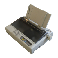
THEORY OF OPERATION
1. Block Diagram
The block diagram of this printer is shown in Fig. 2-1.
Fig. 2-1 Block Diagram
(1) Main Logic Board
This board receives data from the host computer and stores it in the RAM in the order of arrival. The CPU on this
board reads the data from the RAM, and edits it according to the program stored in the ROM.
When the editing is completed, various drive signals from the CPU are sent to the printer mechanism to perform
printing.
<Explanation>
1 CPU M50734SP
• Controls this printer.
2 PROM
• Contains the program which executes control of the printer.
3 EE-PROM BR93C46 46 × 16 bits
• Contains the data (EDS data and so on) in the memory switch.
4 RAM 32K-bytes
• Used as stack area, work area and data buffer of the CPU.
5 Parallel interface
6 Gate array (custom IC)
• Inputs or outputs several signals.
7 Driver
• The data edited by the CPU and gate array are sent to the printer mechanism after conversion to the signal
for the print head drive, carriage motor drive and paper feed motor drive respectively.
(2) Control Panel Board
This panel circuit is for manual operation of the printer.
(3) Printer Mechanism
The printer mechanism consists of a print head, carriage motor, paper feed motor and detectors.
(4) Power Supply Unit
AC power is converted to 25VDC and 5VDC.
 Loading...