5th oor, successively set as 7,8,9..., and if there is no plate in the 3rd and 4th oors, from the
5th oor, successively set as 5,6,7....
Input part
Plug the wiring interface of the lift-locked and fire-emergency switches into the socket of JP1
and JP2, plug the general up/down buttons wiring interface into the JP3 and JP4,, and plug the
disabled up/down buttons wiring interfaces into the JP5 a
nd JP6.
Plug the wiring interface of the MOD-bus communication cable into CN1.
Remark:
Do not set the oor address of the hall call board as 0;a)
The STP is recommended for the communication wiring to avoid the external b)
interference to the communication signal;
It’s recommended to use the shielded cable as the communication signal wire; c)
Please wiring firmly according to the terminal symbol;
d)
Terminal input and button output
Terminal Function
JP1 The pin 2 and 3 of lift-locked switch interface are the pin of switching value, the pine 4 is
the lift-locked lamp output.
JP2 Fire-emergency switch interface, the pin 2 and 3 are the switching value wiring pin, pin 4
is the fire-emergency indicator output
JP3 General up call button interface, the pin 2 and 3 are the switching value wiring pin, the pin
1 and 4 are the power wirin
g pin used for the control of button lamp.
JP4 General down call button interface, the pin 2 and 3 are the switching value wiring pin, the
pin 1 and 4 are the power wiring pin used for the control of button lamp.
JP5 Disabled up call button interface, the pin 2 and 3 are the switching value wiring pin, the
pin 1 and 4 are the power wiring pin used for the control of button lamp.
JP6 Disabled down call b
utton interface, the pin 2 and 3 are the switching value wiring pin, the
pin 1 and 4 are the power wiring pin used for the control of button lamp.
CN1 MOD-bus communication and power wire terminal, 4PIN interface the pin 2 and 3 are the
pin of MOD-bus communication wire, the pin 1 and 4 are the power wiring pin.
CN2 Relay output, see Fig.3-9-3 for the definition details
Table 4 I/O Terminal definition
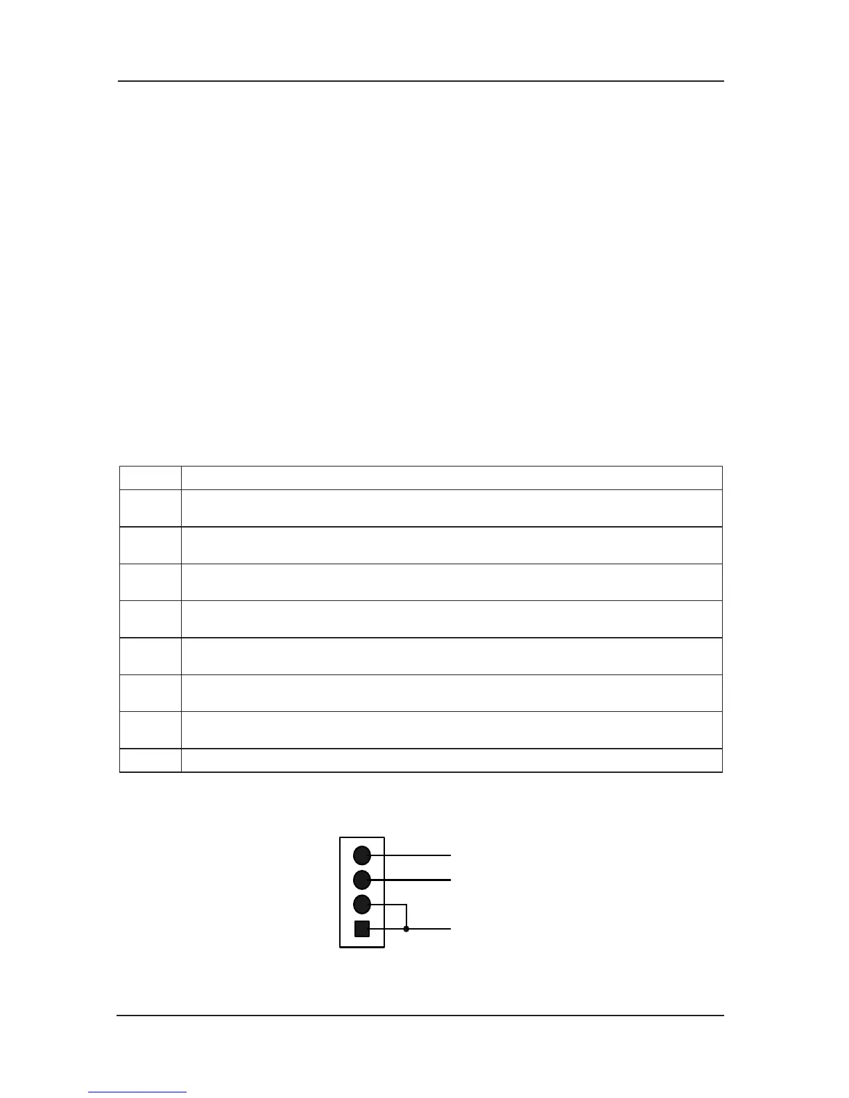
J
P1-JP6 are 4PIN interfaces. The pin details refer to Fig. 3-11
 Loading...