F - 20 Tait Orca vehicle kit June 2003 IPN: M5000-00-105
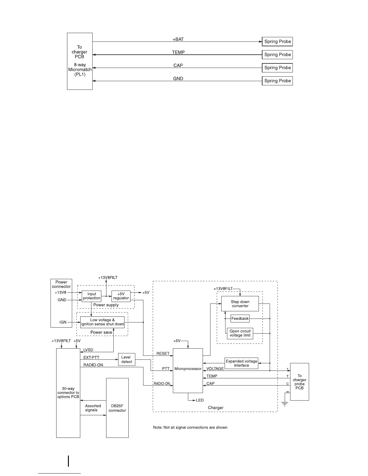
Figure F-11: Vehicle kit charger probe PCB block diagram
Vehicle kit charger probe PCB
(IPN 220-01564-xx)
This PCB provides the interface to the radio
battery for charging and is connected to the
charger PCB via an 8-way MicroMatch ribbon
cable. A block diagram of this PCB is shown in
Figure F-11.
Vehicle kit charger PCB
(IPN 220-01504-xx)
This PCB contains the fast charger circuit
module, the majority of the power supply
module and about half of the power save
module. A block diagram of this board is
shown in Figure F-12.
Current source
The switch mode current source is based
around a Maxim MAX1627 100% duty cycle,
high efficiency, step down DC-DC controller
(IC4). The core of the current source is a Buck
converter consisting of Q9, L2, C46, C47 and
D5. The feedback for the controller (IC4) is via
current sense resistors (R58, R59) and a differ-
ential amplifier (IC5:B).
In steady state, approximately 0.8 A flows
through R58 and R59, generating a voltage
which is amplified by the differential amplifi-
er, IC5:B. The output of this is fed into pin 2 of
IC4 (FB). The threshold of the feedback input
(IC4 pin 2) is 1.3 V, relative to VGND. When
the feedback signal on pin 2 is above 1.3 V, the
controller (IC4) turns off Q9. Similarly, when
the feedback signal is below 1.3 V, the control-
ler turns on Q9.
Figure F-12: Vehicle kit charger PCB block diagram
 Loading...