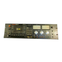
122
3-14-3 Circuits
See
Fig. 3-39.
There
are
three circuits
that
control
the record-
ing bias and equalization characteristics, depend-
ing
on
the
spectrum
of
the
input
signal. These
are the
control
signal
circuit,
the
variable bias
circuit,
and the variable equalizer.
1)
Control
signal
circuit
The recording bias and equalization character-
istics must
be
varied in accordance
with
high-
frequency components
of
the
input
signal and
their
level.
For
this
purpose,
it
is
necessary
to
generate a signal
which
controls
them,
which
is
done
by
detecting and measuring
high-frequency components in the
input
sig-
nal and
their
level.
In the
Dolby
B-type processor
(as
used
in the
M 122), the noise
reduction
control
signal
is
generated
from
the
same
parameters
as
those
used
by
the
Dolby
HX
system. This signal
is
taken
from
pin 14
of
Dolby
N R
IC
U301
(U401) and supplied
to
buffer
amplifiers
U303-a_and U303-b.
a.
U303-a and U303-b select and
output
the
higher
of
the
!\tVo
input
signals
without
permitting
the
Dolby
processors
of
the
left
and
right
channels
to
interfere
with
each
other.
b.
The
output
of
the
buffer
stage
is
applied
to
pin 12
of
high-gain, non-inverting ampli-
fier
U303-c. Generally the DC
output
vol-
tage
of
this
amplifier
rises together
with
the
DC
input
voltage. A
DC
bias voltage ad-
justed
by
semi-fixed resistor R36
or
R37
is
applied
to
pin 13
of
U303-c. This voltage
determines the threshold
of
the
control
voltage where
the
recording bias begins
to
decrease due
to
high-frequency com-
ponents contained in the recording
input
signal. The threshold varies
with
the
type
of
tape; R36 adjusts
for
'normal'
tape
while
R37 adjusts
for
'Co
(Cr02)'
tape.
c.
The
output
of
DC
amplifier
U303-c
is
sent
to
the
selector
circuit
which
generates
conditions
for
Dolby
HX
system operation.
The
output
of
U303-c
is
fed
to
the variable
bias
circuit
and variable equalizer
circuit
only
in the
following
conditions.
NR
SYSTEM
switch:
NR+HX
SPEED
switch:-STANDARD
BIAS switch: Co
(Cr02)
or
NORMAL
2) Variable bias
circuit
The
output
of
the selector
circuit
is applied
to
pin 2
of
U303-d.
a.
U303-d is
an
inverting
amplifier
with
a gain
of
1 using
Vcc/2
as
its reference voltage.
The DC
output
voltage falls (rises)
as
the
DC
input
voltage rises (falls).
The
output
of
U303-d controls the
base
voltage
of
transistor
0303
which
is
located
in series
with
the
power
supply
circuit
of
bias
oscillator
U 1 03.
b.
When the level
of
high-frequency compo-
nents contained in the recording signal
is
high, the DC voltage appfied
to
pin 2
of
U303-d
by
the
control
signal
circuit
rises
and, therefore, the DC
output
voltage
from
pin 1
of
U303-d falls. When the voltage at
pin 1
of
U303-d falls, the
base
voltage
of
0303
falls and its
base
current
decreases.
As a result, the
collector
current
of
0303
decreases,
the
voltage
drop
across the col-
lector and
emitter
increases, and the
volt-
age
supplied
to
bias oscillator
U1
03
falls.
When the supply voltage
to
U103 falls, the
output
of
the
oscillator
falls,
that
is,
bias
is
lowered.
The
minimum
and
fixed
(maxi-
mum) bias levels
are
determined
by
R328
and R329.
3) Variable equalizer
The
output
of
the
control
signal
circuit
is
supplied
to
the variable bias
circuit
and the
variable equalizer simultaneously.
a.
The variable equalizer
is
basically a low-
pass
filter.
A pair
of
variable conductance
amplifiers U302s
are
used
to
provide vari-
able
cutoff
time
constant Tc,
which
is
a
linear
function
of
the
current
flowing
through resistor R335.
b.
When the level
of
high-frequency compo-
nents in the recording signal
is
high, the DC
output
voltage
of
the
control
signal
circuit
rises and
current
flowing
through R335
increases. As a result, variable
cutoff
time
constant
Tc
becomes large and the
tumover
frequency falls.
c. Since the variable equalizer
is
basically a
low-pass
filter,
reduction in
turnover
fre-
quency results in increased attenuation
at
high frequencies. Because
of
this, the re-
cording signal passing through the variable
equalizer varies
as
curves ® and @
shown in Fig. 3-37.
39
 Loading...