Theory of Operation—2465B/2467B Service
Address Decode
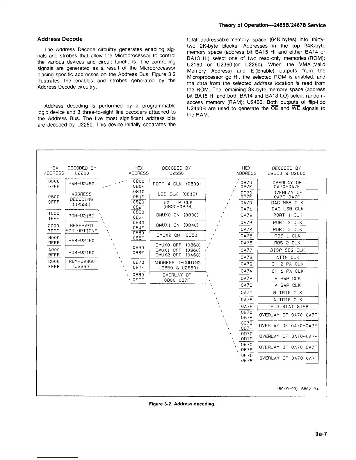
The Address Decode circuitry generates enabling
sig-
nals and strobes that allow the Microprocessor to control
the various devices and circuit functions. The controlling
signals are generated as a result of the Microprocessor
placing specific addresses on the Address Bus. Figure 3-2
illustrates the enables and strobes generated by the
Address Decode circuitry.
Address decoding is performed by a programmable
logic device and 3 three-to-eight line decoders attached to
the Address Bus. The five most significant address bits
are decoded by U2250. This device initially separates the
total addressable-memory space (64K-bytes) into thirty-
two 2K-byte blocks. Addresses in the top 24K-byte
memory space (address bit BA15 HI and either BAM or
BA13 HI) select one of two read-only memories (ROM);
U2160 or U2360(or U2260). When the VMA (Valid
Memory Address) and E (Enable) outputs from the
Microprocessor go HI, the selected ROM is enabled, and
the data from the selected address location is read from
the ROM. The remaining 8K-byte memory space (address
bit BA15 HI and both BAM and BA13 LO) select random-
access memory (RAM); U2460. BotlT_ outputs_of flip-flop
U2440B are used to generate the OE and WE signals to
the RAM.
HEX
ADDRESS
DECODED BY
U2250
HEX
ADDRESS
0000
07FF
0800
0FFF
1000
1FFF
2000
7FFF
8000
9FFF
A000
BFFF
C000
FFFF
RAM-U2460
ADDRESS
DECODING
(U2550)
R0M-U2160
RESERVED
FOR OPTIONS
RAM-U2460
R0M-U2160
R0M-U2360
(U2260)
' 0800
080F
0810
081F
0820
082F
0830
083F
0840
084F
0850
085F
0860
086F
0870
087F
\ 0880
\ 0FFF
DECODED BY
U2550
PORT 4 CLK (0800)
LED CLK (0810)
EXT FP CLK
(0820-0823)
DMUXO ON (0830)
DMUXl ON (0840)
DMUX2 ON (0850)
DMUXO OFF (0860)
DMUXl OFF (0960)
DMUX2 OFF (0A60)
ADDRESS DECODING
(U2650 S U2660)
OVERLAY OF
0B00-087F
HEX
ADDRESS
/ 0870
087F
0970
097F
0A70
0A71
0A72
0A73
0A74
0A75
0A76
0A77
0A78
0A79
0A7A
0A7B
0A7C
0A7D
0A7E
0A7F
0B70
0B7F
0C70
0C7F
0D70
0D7F
0E70
N
0E7F
-
0F70
0F7F
DECODED BY
U2650 S U2660
OVERLAY OF
0A70-0A7F
OVERLAY OF
0A70-0A7F
DAC MSB CLK
DAC LSB CLK
PORT 1 CLK
PORT 2 CLK
PORT 3 CLK
ROS 1 CLK
R0S 2 CLK
DISP SEQ CLK
ATTN CLK
CH 2 PA CLK
CH 1 PA CLK
B SWP CLK
A SWP CLK
B TRIG CLK
A TRIG CLK
TRIG STAT STRB
OVERLAY OF 0A70-0A7F
OVERLAY OF 0A70-0A7F
OVERLAY OF 0A70-0A7F
OVERLAY OF 0A70-0A7F
OVERLAY OF 0A70-0A7F
(6019-09) 6862-34
Figure 3-2. Address decoding.
3a-7