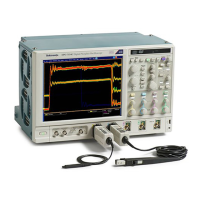
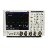
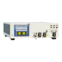
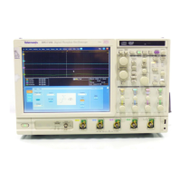
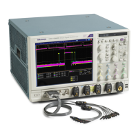
Specifications (MSO70000/C Series, DSA/DPO70000B/C Series, and DPO7000 Series)
Table 1-1: Channel input and vertical s pecifications, all MSO70000/C, DSA/DPO70000B/C, and DPO7000 Series
models (cont.
)
Characteri
stic
Descriptio
n
Input resistance,
≥ 4 GHz models
100 mV FS to 995 mV FS: 50 Ω ±1.5% at 25 ºC (77 ºF)
50 Ω ± 2% over 10 to 45 ºC (50 to 113 ºF), type tested
1 V FS to 5 V FS: 50 Ω ±2.2 Ω over 10 to 45 ºC (50 to 113 ºF), type tested
Input impedance, DC coupled,
< 4 GHz models
1MΩ, DC coupled 1 MΩ ±1%inparallelwith13pF±2pF
50 Ω, DC coupled 50 Ω ±1%,typical
<1 V
RMS
for <1.0 V/Full Scale settings
Maximum input voltage,
≥ 4 GHz models
<5.0 V
RMS
for ≥ 1.0 V/Full Scale settings
Maximum input voltage,
< 4 GHz models
1MΩ – DC coupled,
1MΩ – AC coupled, or GND
coupled
150 V. Derate at 20 dB/decade to 9 V
RMS
above 200 kHz.
The maximum input voltage at the BNC, between center conductor and ground is 400 V peak.
The RMS voltage is limited to <150 V for arbitrary waveshapes including DC. The maximum
pulse width for impulses with peaks over 150 V i s 50 μs. Example: At 0 V to 400 V peak,
rectangular wave, the duty factor is 14%.
The m aximum transient withstand voltage is ± 800 V peak.
50Ω 5 V RMS, with peaks ≤ ±24V
Input VSWR, typical
≥ 4 GHz models
Input Frequency
VSWR < 1 V/Full Scale VSWR ≥ 1V/FullScale
1.25
1.5
2.1
2.5
3.2
1.2
1.2
1.5
1.5
1.9
<2.5 GHz
<6 GHz
<14 GHz
<15 GHz
<20 GHz
Measured with a TekConnect SMA adapter and a network analyzer
< 4 GHz models f
in
<3.5 GHz
f
in
<2.5 GHz
f
in
<2 GHz
f
in
<1 GHz
3.0
2.0
1.5
1.2
Number of digitized bits
8bits
Digitizer nonlinearity, typical
< 1.0 DL (digitization level), differential; < 1 DL integral, independently based
1–2 MSO70000/C, DSA70000B/C, DPO7000B/C, DPO7000, MSO5000, DPO5000 Series
 Loading...
