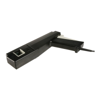
Theory of operation
Probe input architecture
P7700 Series pr
obes feature a new probe architecture that addresses the need
for high frequency response with decreased probe loading for high-speed, low
power applications such as MIPI® and LPDDR. High p erformance probes with
multi-GHz bandwidth have evolved in recent years, starting from traditional
designs with metal pin tips attached to a probe head amplifier located at the end of
a coaxial cable. As the probe bandwidth extended to 10 GHz and above, probe
designs mig
rated to connectorized amplifier input structures that supported a
variety of high frequency passive probe tips, including solderable tip designs.
These probe tips typically provide a passive input attenuator network at the
probe tip followed by a long cable attached to the probe amplifier connection
socket. Although these passive tip, probe designs enable good, high frequency
performance, they show higher probe loading in the frequency band below 1 GHz
than earl
ier traditional designs with an amplifier closer to the probe tip. A probe
with this higher loading characteristic below 1 GHz has problems when taking
measurements of signals such as MIPI that can be switched to an unterminated,
high impedance mode for low power operation. The P7700 Series probe solves
this loading problem by introducing an active probe tip design with a tiny
buffer amplifier located near the tip inputs. By locating an amplifier with a h igh
imped
ance attenuator network at the probe tip inputs, the p robe tip parasitic
capacitance can be kept much lower than passive cable tip designs, thus reducing
probe loading in the low power signaling frequency band used by serial data
standards such as MIPI.
The following figure shows a simplified diagram of the P7700 Series active
probe tip architecture.
Figure 3: P7700 Series TriMode probe input architecture
P7700 Series TriMode Probes Technical Reference 5
 Loading...