Theory of operation
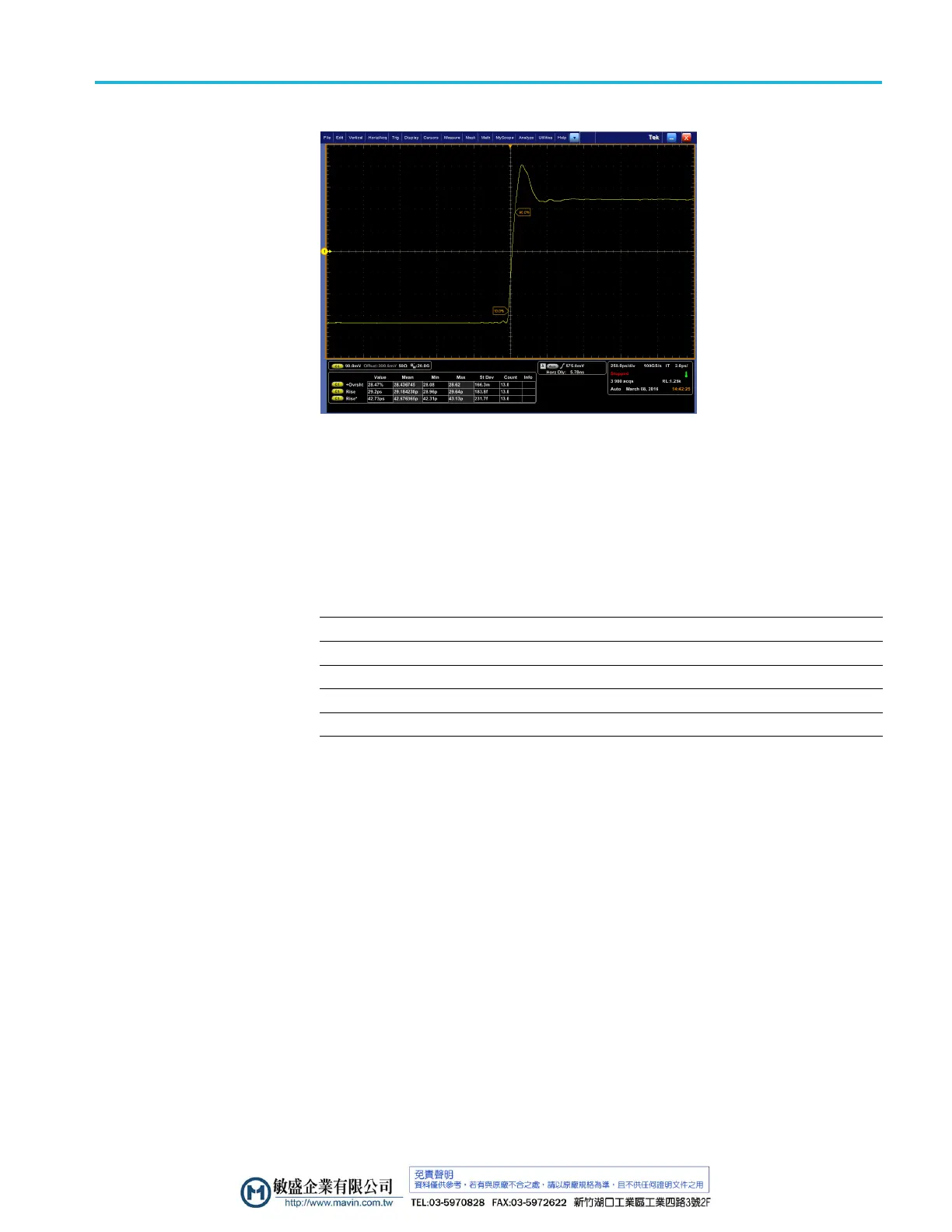
Figure 17: P77STFLXA solder tip attached with 300 mils (7.62 mm) wires (rise time =
42.8 ps)
The following table shows the rise time and overshoot degradation versus l ead
length.
Table 2: Rise time and overshoot degradation versus lead length
Signal wire lead
length 10 - 90 Rise time 20 - 80 Rise time
Effective
bandwidth
0.25 mm 30.5 ps 21 ps
20 GHz
1.90 mm 27.9 ps 19.3 ps
20 GHz
3.05 mm 30.1 ps 20.9 ps
20 GHz
5.08 mm 34 ps 23.6
17 GHz
7.62 mm 42.8 ps 29.2
14 GHz
Using offset voltag e to
extend P770 0 series
solder-in tip input voltage
range
The single-ended linear dynamic range of the TekFlex solder-in tip inputs is
specified to be 2.5 V
p-p
, which is a range from -1.25 V to +1.25 V with zero
volt offset. The dynamic range of P7700 Series buffers is limited by the input
attenuation factor, which is 2X for the solder-in probe tips as shown in the
following simplified figure. A 2X attenuation factor was selected for the probe
tips to o ptimize dynamic range and noise, since a higher attenuation factor would
have increased probe noise. Although the dynamic range of the probe tip buffer
cannot be extended, it is possible to extend the range over which the tip dynamic
range window can be moved by adjusting the probe offset voltage. The offset
voltage range o f the TekFlex solder-in tips is -4 V to +4 V, which is adjusted using
the Probe Setup screen of the oscilloscope or the offset knobs on the oscilloscope
front panel. Using the offset voltage controls, it is possible to make measurements
within any 2.5 V
p-p
window between -5.25 V and +5.25 V. As an example, by
setting the offset voltage to +3.0 V, it is possible to measure an HDMI signal,
which has a signal swing between about +2.8 V and +3.3 V.
P7700 Series TriMode Probes Technical Reference 25
 Loading...