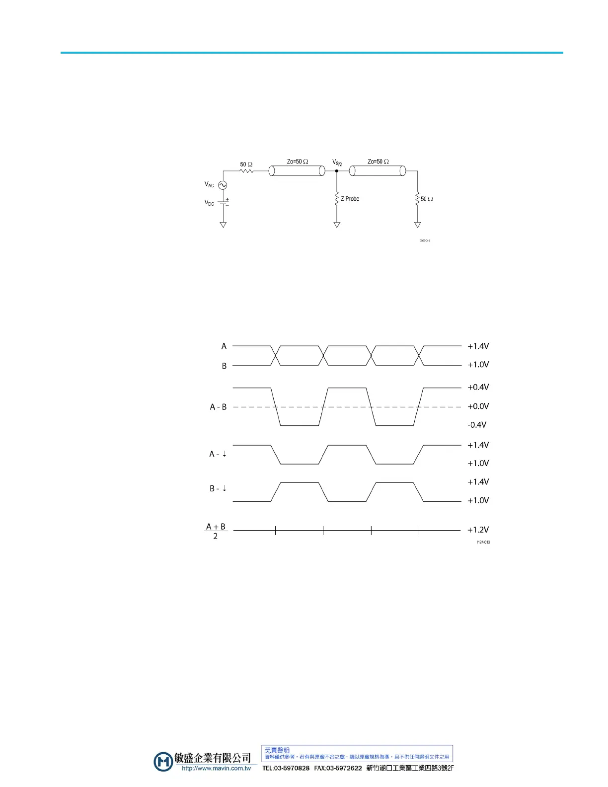
Theory of operation
The input imped
ance for a solder tip, Z probe, varies with frequency. For a
P77STxxxx tip the DC input resistance is about 50 kΩ and decreases with
frequency above about 10 MHz to about 100 Ω above 10 GHz. Refer to the
graphs later in this document for input impedance information. (See page 43,
Input impedance graphs.)
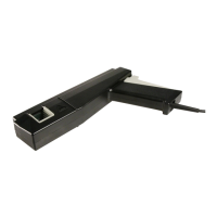
Figure 20: Solder tip measurement configuration
Skew measurements of
differential signals
Differential signals are composed of two complementary single-ended signals
that generally swing around a common bias voltage. An example of an LVDS
differ
ential signal is shown in the following figure.
Figure 21: Example of LVDS differential signal
The complementary single-ended signals labeled A and B in the previous figure
must have well matched signal timing (for example, low skew) to function as
a
useful differential signal. If the signal skew becomes comparable in size to
the rise time of the complementary signals, then the rise time of the resulting
differential signal will be slower than expected. Skew is a measure of the time
delay mismatch b etween two suppos edly matched signals.
P7700 Series TriMode Probes Technical Reference 29
 Loading...