Theory of operation
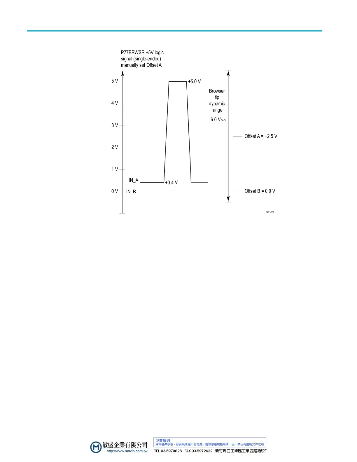
Figure 19: Differential input mode signal voltage and offset voltage
The configuration process described in this section maximizes the a vailable
dynamic range of the P77BRWSR tip when making single-ended measurements.
Temperature
compensation
The P7700 Series probes employ temperature compensation to optimize
measurement accuracy. Whenever a probe setting is changed, such as Input
Mode, offset voltage, or vertical scale factor, a temperature compensation update
occurs. Continuous temperature compensation is not done to avoid introducing
noise into the probe amplifiers.
To maximize measurement accuracy when the probe is first powered on from a
cold start condition, you must allow a 20 minute warm-up period for the probe
and oscilloscope. After the warm-up period, you should adjust or toggle a probe
setting, such as the vertical scale factor, to trigger the temperature compensation
update.
Otherwise, a cold tempe rature compensation value might be used, which
would result in a small gain error.
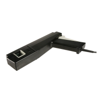
Solder tip measurement
configuration
In many of the high-frequency signaling standards that the P7700 Series probes
are designed for, a 50 Ω termination at the transmitter is in parallel with another
50 Ω termination at the end of the transmission line path, effectively making
a25Ω signal source impedance. In this application, the solder tip adapter
measurement configuration is designed to pick off the transmitted signal at a
location in the signal transmission path.
28 P7700 Series TriMode Probes Technical Reference
 Loading...