Table of Contents
List of Figure
s
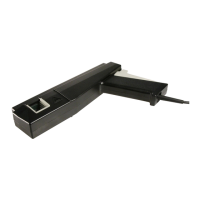
Figure 1: P7700 Series TriMode probe components ........................................................... 1
Figure 2: P7
700 Series TriMode active probe tips.............................................................. 4
Figure 3: P7700 Series TriMode probe input architecture..................................................... 5
Figure 4: TriMode input structure ............................................................................... 11
Figure 5: P7700 probe tip inputs................................................................................. 12
Figure 6: Operating voltage window (TekFlex solder-in tips)................................................ 13
Figure 7: Dynamic range versus linearity at the probe amplifier step gain settings........................ 15
Figure 8:
Operating voltage window (P77BRWSR)........................................................... 16
Figure 9: Dynamic range linearity error plot ................................................................... 16
Figure 10: Simplified diagram of the P7700 Series probe tip input network ............................... 18
Figure 11: Probe setup screen.................................................................................... 19
Figure 12: Simplified Auto Offset circuitry .................................................................... 20
Figure 13: P77STFLXA solder tip attached with 10 mils (0.250 mm) wires (rise time = 30.5 ps) ...... 23
Figur
e 14: P77STFLXA solder tip attached with 75 mils (1.90 mm) wires (rise time = 27.9 ps) ........ 23
Figure 15: P77STFLXA solder tip attached with 120 mils (3.05 mm) wires (rise time = 30.1 ps) ...... 24
Figure 16: P77STFLXA solder tip attached with 200 mils (5.08 mm) wires (rise time = 34 ps)......... 24
Figure 17: P77STFLXA solder tip attached with 300 mils (7.62 mm) wires (rise time = 42.8 ps) ...... 25
Figure 18: Simplified diagram of the P7700 Series probe tip input network ............................... 26
Figure 19: Differential input mode signal voltage and offset voltage ....................................... 28
Fi
gure 20: Solder tip measurement configuration.............................................................. 29
Figure 21: Example of LVDS differential signal............................................................... 29
Figure 22: Simplified model of a differential amplifier ....................................................... 33
Figure 23: Typical CMRR........................................................................................ 34
Figure 24: Typical channel isolation ............................................................................ 36
Figure 25: P77STCABL differential impedance............................................................... 43
Figure 26: P77STCABL SE impedance ........................................................................ 43
Figure 27: P77STFLXA differential impedance ... .... .................. ...................... ................ 44
Figure 28: PST77FLXA SE impedance......................................................................... 44
Figure 29: P77BRWSR differential impedance ................................................................ 45
Figure 30: Differential mode P77STCABL and P77FLXA equivalent circuit diagram ................... 45
Figure 31: Single-ended P77FLXA equivalent circuit diagram.............................................. 45
Figure 32: P77BRWSR equivalent circuit diagram with 50 mil spacing.................................... 46
Figure 33: P77BRWSR equivalent circuit diagram with 200 mil spacing .................................. 46
ii P7700 Series TriMode Probes Te chnical Reference
 Loading...