PP_5V0, the pulldown is turned off. The load on VBUS will then continue to pull VBUS down until the ideal diode
switch structure turns on connecting it to PP_5V0. When switching from PP_HV or PP_EXT to PP_5V0, PP_HV
or PP_EXT must be above VSO_HV to follow the switch-over shown in Figure 9-26.
PP_5V0 VBUS
Fast
current
limit
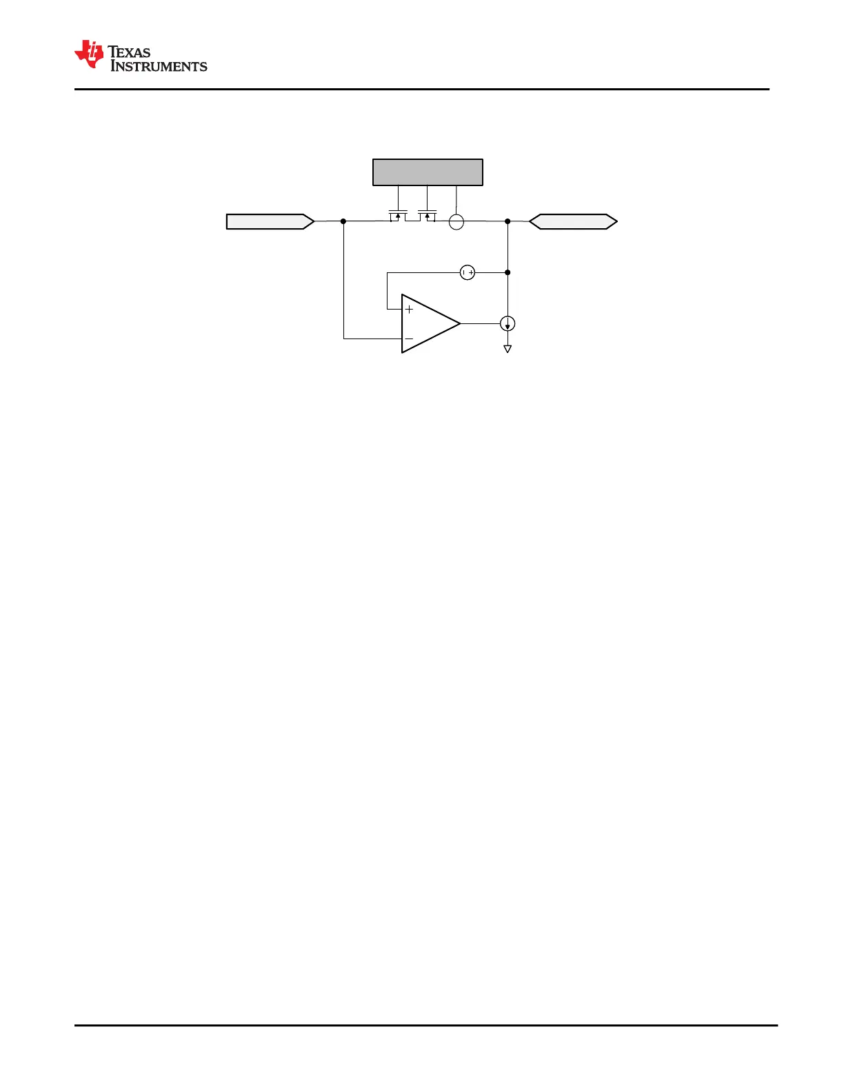
PP_5V0 Gate Control
and Current Limit
VHVDISPD
Slew Rate
Controlled
Pulldown
Figure 9-27. PP_5V0 Slew Rate Control
9.3.3.20 VBUS Transition to VSAFE0V
When VBUS transitions to near 0 V (VSAFE0V), the pulldown circuit in Figure 9-27 is turned on until VBUS
reaches VSAFE0V. This transition will occur within time TSAFE0V.
9.3.3.21 C_CC1 and C_CC2 Power Configuration and Power Delivery
The C_CC1 and C_CC2 pins are used to deliver power to active circuitry inside a connected cable and output
USB-PD data to the cable and connected device. Figure 9-11 shows the C_CC1, and C_CC2 outputs to the port.
Only one of these pins will be used to deliver power at a time depending on the cable orientation. The other pin
will be used to transmit USB-PD data through the cable to a connected device.
Figure 9-28 shows a high-level flow of connecting these pins based on the cable orientation. See the Section
9.3.2 section for more detailed information on plug and orientation detection.
www.ti.com
TPS65982
SLVSD02E – MARCH 2015 – REVISED AUGUST 2021
Copyright © 2021 Texas Instruments Incorporated
Submit Document Feedback
49
Product Folder Links: TPS65982