in Port Data Multiplexer Requirements and Characteristics. RPU_EP is disconnected during transmit mode of
the transceiver.
When the endpoint is in receive mode, the resistance RPU_EP is connected to the D– pin of the top or bottom
port (C_USB_TN or C_USB_BN) depending on the detected orientation of the cable. The RPU_EP resistance
advertises low speed mode only.
9.3.4.8 Battery Charger (BC1.2) Detection Block
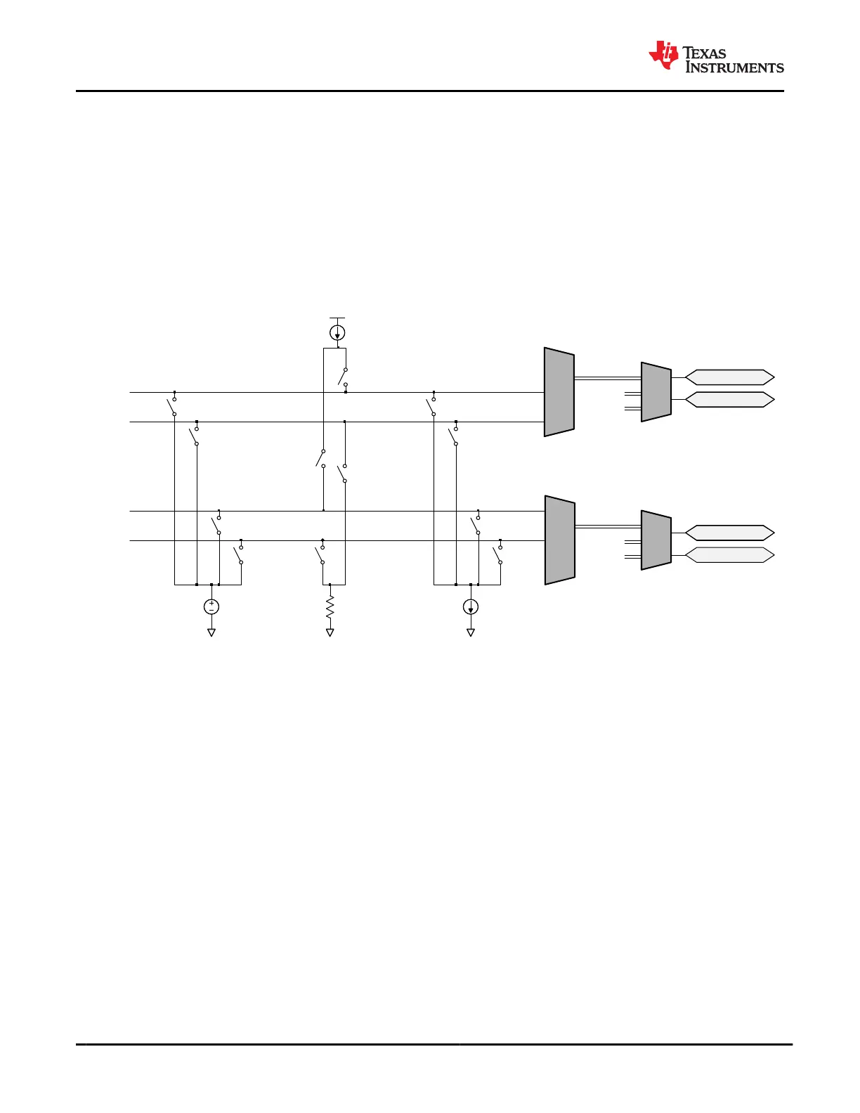
The battery charger (BC1.2) detection block integrates circuitry to detect when the connected entity on the USB
D+/D– pins is a charger. To enable the required detection mechanisms, the block integrates various voltage
sources, currents, and resistances to the Port Data Multiplexers. Figure 9-39 shows the connections of these
elements to the Port Data Multiplexers.
USB_EP
USB_RP
VDX_SRC IDX_SNK
USB_EP
USB_RP
RDM_DWN
IDP_SRC
VLGC_HI
To ADC
To ADC
C_USB_TP
C_USB_TN
C_USB_BP
C_USB_BN
Figure 9-39. BC1.2 Detection Circuitry
9.3.4.9 BC1.2 Data Contact Detect
Data Contact Detect follows the definition in the USB BC1.2 specification. The detection scheme sources a
current IDP_SRC into the D+ pin of the USB connection. The current is sourced into either the C_USB_TP (top)
or C_USB_BP (bottom) D+ pin based on the determined cable/device orientation. A resistance RDM_DWN is
connected between the D– pin and GND. Again, this resistance is connected to either the C_USB_TN (top) or
C_USB_BN (bottom) D– pin based on the determined cable/device orientation. The middle section of Figure
9-39, the current source IDP_SRC and the pulldown resistance RDM_DWN, is activated during data contact
detection.
9.3.4.10 BC1.2 Primary and Secondary Detection
The Primary and Secondary Detection follow the USB BC1.2 specification. This detection scheme looks for a
resistance between D+ and D– lines by forcing a known voltage on the first line, forcing a current sink on the
second line and then reading the voltage on the second line using the general purpose ADC integrated in the
TPS65982. To provide complete flexibility, 12 independent switches are connected to allow firmware to force
voltage, sink current, and read voltage on any of the C_USB_TP, C_USB_TN, C_USB_BP, and C_USB_BN.
The left and right sections of Figure 9-39, the voltage source VDX_SRC and the current source IDX_SNK, are
activated during primary and secondary detection.
TPS65982
SLVSD02E – MARCH 2015 – REVISED AUGUST 2021
www.ti.com
58 Submit Document Feedback
Copyright © 2021 Texas Instruments Incorporated
Product Folder Links: TPS65982